Sequential Lamination & Stacked Vias
Sequential Lamination Overview
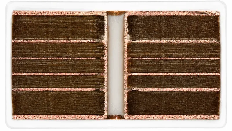
What Is Sequential Lamination?
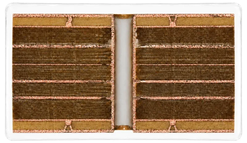
Benefits of Sequential Lamination
Sequential Lamination Considerations
Stacked Vias Overview
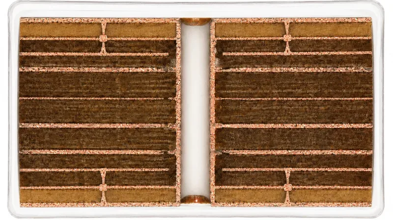
Stacked vias are commonly used in HDI PCBs to create vertical electrical connections between multiple layers. By placing microvias directly above one another, they support higher routing density and more compact PCB designs.
What Is a Stacked Via?
A stacked via consists of two or more vias positioned directly above one another across multiple PCB layers. The vias are formed and copper-plated during sequential lamination to create a continuous vertical electrical connection.
Benefits of Stacked Vias
Stacked Via Considerations
Applications for Sequential Lamination and Stacked Vias
Relationship Between Sequential Lamination and Stacked Vias
Sequential Lamination and Stacked Via Support
Topline Circuit supports sequential lamination and stacked via structures for complex multilayer and HDI PCBs. Our engineering team reviews the stack-up, via structure, layer connections, materials, and manufacturing requirements before production. This helps identify design risks and confirm that the proposed structure is suitable for fabrication.
Send us your Gerber files, stack-up, and via requirements for review.
Your Sequential Lamination and Stacked Via Manufacturer
With more than 15 years of PCB manufacturing experience, Topline Circuit supports sequential lamination and stacked via structures for complex multilayer and HDI boards. Our services cover PCB fabrication, assembly, component sourcing, and engineering support, helping customers manage projects through one supplier.We review the stack-up, via structure, materials, and production requirements before manufacturing to reduce design risks and improve production reliability.