Sequential Lamination & Stacked Vias
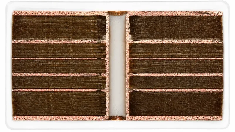
Multilayer PCB cross-section showing copper layers and plated through-hole

Sequential Lamination Overview

Sequential lamination is a key process in advanced PCB manufacturing. It is commonly used for high-density interconnect (HDI) boards, allowing more layers, microvias, and connections in a compact design.

What Is Sequential Lamination?

Sequential lamination is a PCB manufacturing process used to build complex HDI boards. Copper and dielectric layers are added, laminated, drilled, and plated in multiple stages. This process supports microvias, higher layer counts, and dense interconnections within a compact PCB.

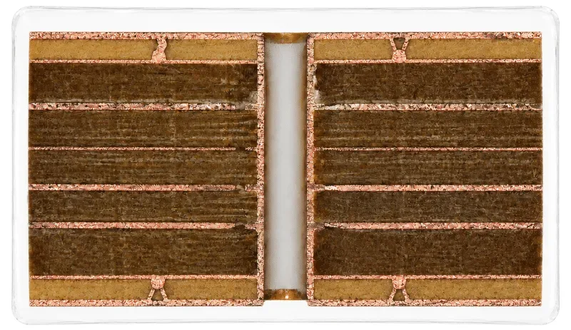
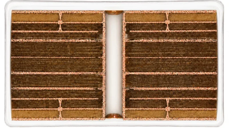
HDI PCB cross-section with sequential lamination and stacked microvias

Sequential Lamination Process

Build the Base Structure

Begin with a PCB core or sub-laminate containing the initial copper layers and circuit patterns.

Drill and Plate

Drill precise holes through the structure and plate them with copper to create electrical connections between layers.

Add New Layers

Add dielectric material and copper foil to form the next layer of the PCB.

Laminate the Layers

Apply controlled heat and pressure to bond the new materials to the existing structure.

Form and Plate Vias

Drill or laser-form vias in the newly added layer, then plate them to establish the required connections.

Repeat the Cycle

Repeat the layering, lamination, drilling, and plating steps until the required layer count and interconnection structure are complete.

Benefits of Sequential Lamination

  • Higher interconnection density: Supports complex routing and more electrical connections within a limited board area.
  • Compact PCB designs: Enables microvias and fine-pitch features that reduce the space required for interconnections.
  • Greater design flexibility: Allows designers to create complex HDI stack-ups for specific electrical and mechanical requirements.

Sequential Lamination Considerations

Stacked Vias Overview

Stacked vias are commonly used in HDI PCBs to create vertical electrical connections between multiple layers. By placing microvias directly above one another, they support higher routing density and more compact PCB designs.

What Is a Stacked Via?

A stacked via consists of two or more vias positioned directly above one another across multiple PCB layers. The vias are formed and copper-plated during sequential lamination to create a continuous vertical electrical connection.

Multilayer PCB cross-section showing copper layers and plated through-hole

Making a Stacked Via

Build the Base Structure

Begin with a PCB core or sub-laminate that contains the initial copper layers and plated connections.

Add the Dielectric and Copper

Add a dielectric layer and copper foil to the existing structure as part of the sequential lamination process.

Laminate the New Layer

Use controlled heat and pressure to bond the new dielectric and copper to the existing PCB structure.

Laser-Drill the Microvia

Use a laser to form a microvia in the newly added dielectric directly above the via below.

Plate and Repeat

Plate the microvia with copper to create the electrical connection. Repeat the cycle until the required stacked-via structure is complete.

Benefits of Stacked Vias

  • Higher routing density: Stacked vias create vertical connections across multiple PCB layers, leaving more space for traces and components.
 
  • Smaller PCB designs: Their compact structure supports fine-pitch components and dense HDI layouts without increasing the board size.
 
  • Shorter connection paths: Direct vertical connections can reduce routing distances between layers and simplify complex interconnections.

Stacked Via Considerations

Applications for Sequential Lamination and Stacked Vias

Sequential lamination and stacked vias are commonly used in compact, multilayer PCBs that require high routing density. Typical applications include:

Relationship Between Sequential Lamination and Stacked Vias

Sequential lamination and stacked vias are closely related, but they are not separate alternatives.

Sequential lamination is the manufacturing process used to add, drill, plate, and bond PCB layers in multiple cycles. It supports complex HDI structures, including blind vias, buried vias, and microvias.

Stacked vias are a specific via structure created during these lamination cycles. Two or more microvias are aligned vertically to form a direct connection across multiple layers.

In short, sequential lamination describes how the PCB is built, while stacked vias describe one of the interconnection structures that the process can produce.

Sequential Lamination and Stacked Via Support

Topline Circuit supports sequential lamination and stacked via structures for complex multilayer and HDI PCBs. Our engineering team reviews the stack-up, via structure, layer connections, materials, and manufacturing requirements before production. This helps identify design risks and confirm that the proposed structure is suitable for fabrication.

Send us your Gerber files, stack-up, and via requirements for review.

HDI PCB cross-section with sequential lamination and stacked microvias

Your Sequential Lamination and Stacked Via Manufacturer

With more than 15 years of PCB manufacturing experience, Topline Circuit supports sequential lamination and stacked via structures for complex multilayer and HDI boards. Our services cover PCB fabrication, assembly, component sourcing, and engineering support, helping customers manage projects through one supplier.We review the stack-up, via structure, materials, and production requirements before manufacturing to reduce design risks and improve production reliability.
Need a PCB Quote?

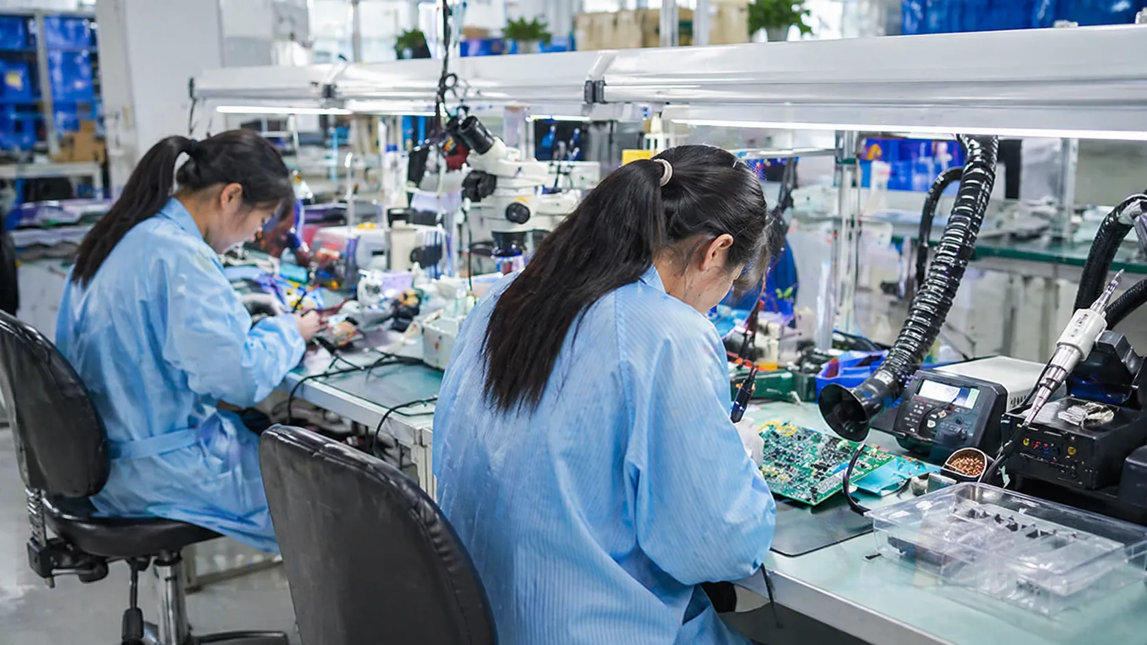
Technicians supporting metal core PCB manufacturing and assembly

Ready to Start Your Project ?

Send us your files. We can help with PCB layout, fabrication, and assembly.