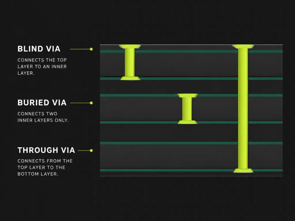
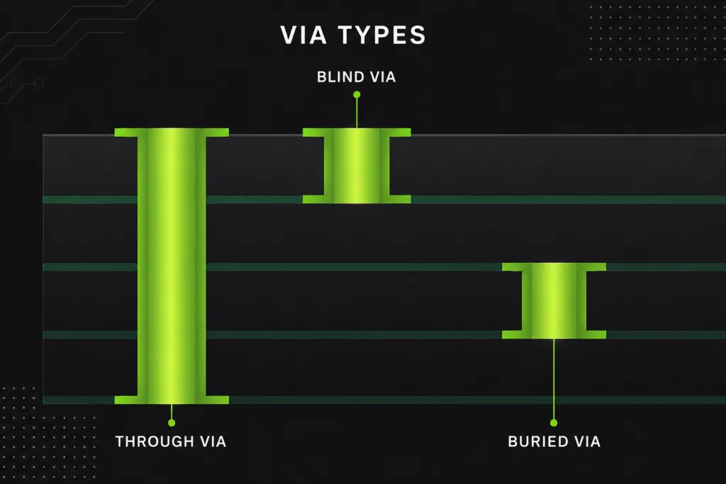
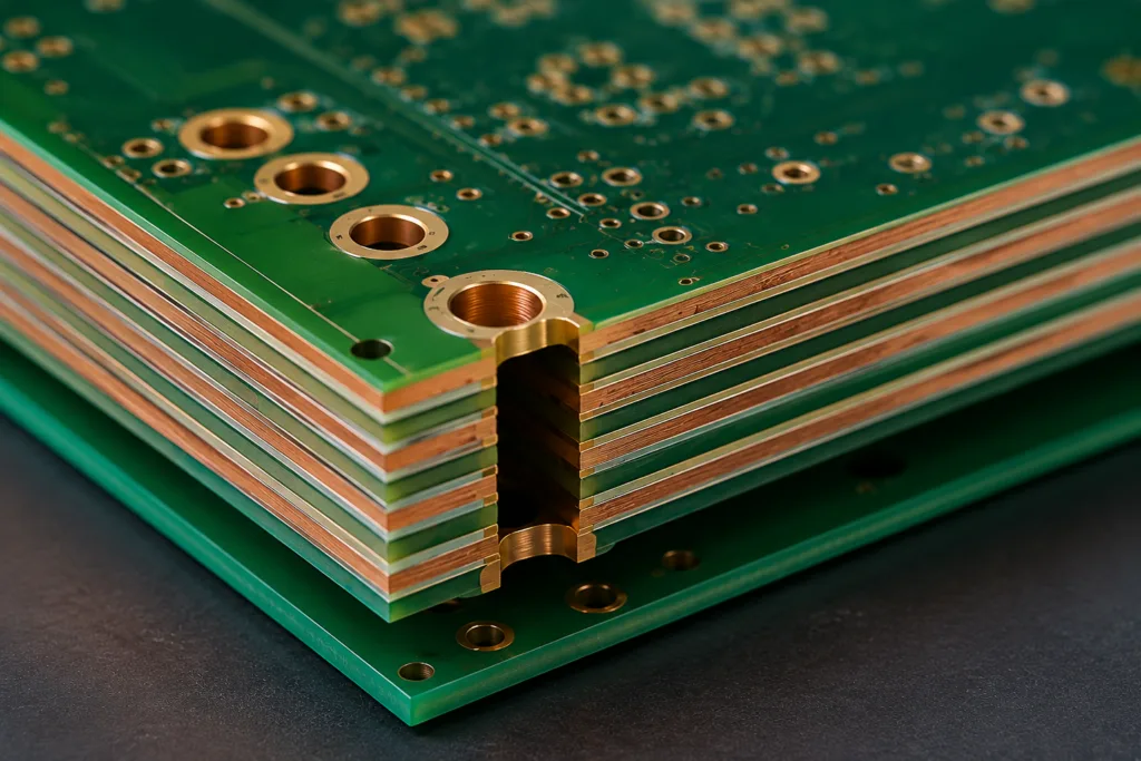
Copper & Epoxy Filled Vias
Copper Microvia and Epoxy Filled Via PCBs
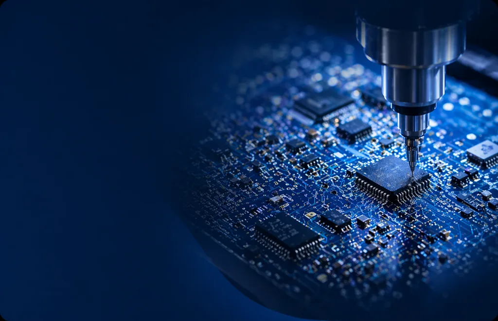
DFYC supports advanced PCB fabrication with copper microvia and epoxy filled thru-vias. These processes are useful for compact, high-density PCB designs.
Filled vias can help improve routing space, support micro BGAs, and make complex PCB layouts easier to manufacture. They can be plated with copper or filled with epoxy, depending on the project requirements.
From PCB layout review to fabrication and assembly, DFYC provides engineering support for compact components, high-density designs, and reliable PCB production.
Overview of Copper Filled Microvias
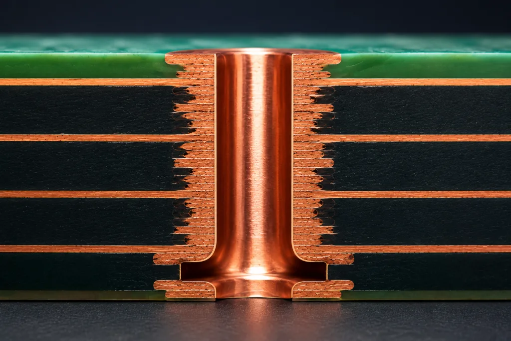
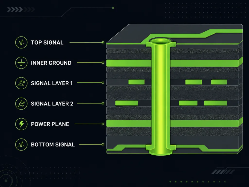
Copper filled microvias are small laser-drilled holes in a PCB. They are filled with copper to improve electrical and thermal performance.
Their main functions include:
- Cooling: copper filled microvias help dissipate heat more effectively.
- Connectivity: they connect different layers inside a circuit board.
Copper filled microvias are usually made by laser drilling. After drilling, the holes are metalized with an electroless copper seed layer. Then the board goes through imaging and specialized electroplating to fill the microvias with copper.
This process requires high precision and careful process control. Because of the extra manufacturing steps, copper filled microvias may increase PCB fabrication costs.
Overview of Epoxy Filled Vias
Epoxy filled vias are thru-holes in a PCB that are filled with epoxy resin. The epoxy resin can be non-conductive or conductive, depending on the design requirements.
Epoxy filled vias are commonly used for:
- Component placement: they allow components to be mounted directly over the via.
- Smooth surface: they help create a flat PCB surface for fine-pitch and compact components.
- Thermal support: conductive epoxy resin can help transfer heat from components such as sensors or GaN amplifiers.
The production process usually starts by plating the hole. Then the via is filled with epoxy. After that, the surface is sealed with copper, often called the cap layer.
Epoxy filled vias are a flexible option for high-density PCB designs. However, standard epoxy does not conduct heat as well as copper or conductive epoxy via fill. So material selection is important when the design needs better thermal performance.
Similarities and Differences Between Copper and Epoxy Filled Vias
Copper filled vias and epoxy filled vias both help improve PCB design. They are used to connect different layers of a circuit board and support more reliable PCB routing.
Both options are common in high-density PCB designs and HDI PCB applications. They help save space, improve layer-to-layer connection, and support compact component placement.
Copper filled microvias are often used for high-density components, such as BGAs and micro BGAs. They help fan out traces to the layer below. They can also channel heat to plane layers and move heat toward the edge of the board. This makes copper filled vias useful for thermal management and high-density interconnect designs.
Epoxy filled vias can be filled with non-conductive or conductive epoxy resin. They are useful when the PCB needs a flat surface. This is important for via-in-pad designs, where components are placed directly over the via.
Epoxy filled vias can also help save space in compact device designs. They are a good choice for small products that need stable PCB layout, reliable routing, and smooth PCB surfaces.
In simple terms, copper filled vias are better for heat transfer and high-density connections. Epoxy filled vias are better for flat surfaces, via-in-pad component placement, and compact PCB layouts.
Filled Via PCB Applications
Filled via PCBs are used in many industries because they support compact layouts, reliable connections, and stable performance. They are especially useful for high-density PCB designs and complex electronic products.
Common applications include:
Telecommunications
Filled via PCBs helps support effective signal transmission and reliable high-frequency performance.
Aerospace
They help improve durability and performance in challenging environments.
Medical Devices
Filled vias support complex PCB layouts and stable performance for advanced medical electronics.
Automotive
They are used in automotive electronics to improve reliability, performance, and space efficiency.
Consumer Electronics
Filled via PCBs helps create smaller and thinner products without reducing performance.
Industrial Electronics
They support robust electronic performance for industrial control systems and equipment.
Energy
Filled via PCBs helps meet the needs of energy applications that require reliable and complex circuitry.
Copper and Epoxy Filled Via Lead Times
PCB lead time depends on design complexity. Filled vias add extra process steps so that they may increase production time.
Copper filled vias and epoxy filled vias usually require filling, curing, plating, inspection, and quality control.
In many cases, each filled via design requirement may add about three days to the production schedule.
To avoid delays, it is best to confirm filled via requirements early before production.
DFYC’s Expertise in Copper and Epoxy Filled Vias
With over 25 years of hands-on experience, DFYC supports copper filled vias and epoxy filled vias for durable, high-performance PCBs.
We help customers improve PCB reliability, support compact layouts, and meet the needs of different industries.
DFYC Is Your Copper and Epoxy Filled
Vias Manufacturer
Choosing the right PCB manufacturer is important for copper microvias and epoxy filled vias. DFYC provides reliable support for filled via PCB projects that require precision, stable quality, and strong engineering experience.
Our engineers understand copper filled vias, epoxy filled vias, PCB stack-up, via structure, material selection, and design for manufacturability. We work with customers to review project requirements and choose the right process.
Copper filled vias are useful when the PCB needs better heat dissipation and high-density connections. Epoxy filled vias are a good choice when the design needs a flat surface, via-in-pad support, or compact component placement.
With advanced equipment and experienced engineering support, DFYC helps customers build durable and high-performance PCBs for different industries and applications.
Client Testimonials
Get started?
Submit a form with your project details, including design specifications, quantity, and any special requirements. We’ll take care of the rest.

Need More Info?
Contact us to discuss your next PCB project.