Heavy Copper PCBs

Why Use Heavy Copper PCBs?
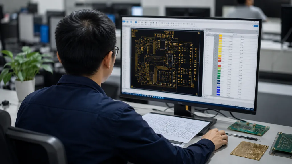
PCB designs should be reviewed carefully before production because later changes can increase costs and delay the project. Heavy copper PCBs require particular attention to copper weight, trace width, spacing, stack-up, and heat management.

High-current circuits need enough copper cross-sectional area to carry the required current without excessive temperature rise. Designers may use thicker copper, wider traces, or both. This is why heavy copper PCBs are commonly used in power electronics and other high-current applications.

10oz Copper PCB
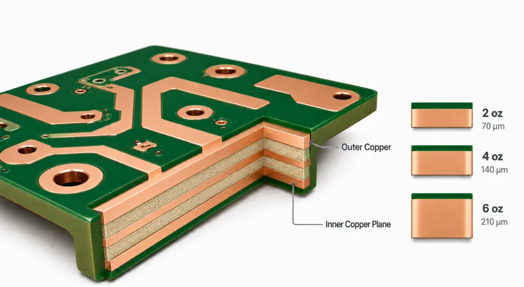
Heavy copper PCB with 2 oz to 6 oz copper layer cross-section

What Is a Heavy Copper Printed Circuit Board?

A heavy copper PCB uses thicker copper layers than a standard PCB to support higher current, better heat management, and greater mechanical strength. Copper thickness is commonly measured in ounces per square foot, with 1 oz equal to approximately 35 μm.

Standard PCBs often use 1 oz or 2 oz copper, while heavy copper PCBs generally use 3 oz or more. The required copper weight depends on the current load, trace width, temperature rise, board structure, and application requirements.

Heavy Copper PCB Applications

Heavy copper PCBs are used in high-current and high-power applications that require reliable current carrying capacity, heat management, and mechanical strength.

Common applications include:

Heavy copper can be used in many PCB designs, but the copper weight should be selected from the current load, trace width, temperature rise, and available board space.

Heavy Copper PCB Construction

Heavy copper PCBs use many of the same etching and plating processes as standard PCBs. However, thicker copper requires greater dielectric spacing between the copper layers. This dielectric is the nonconductive material that separates the layers and provides electrical insulation.

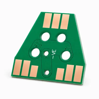
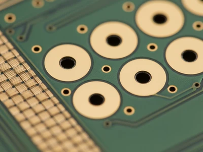
Heavy copper PCB with wide copper pads for high-current applications

Benefits of Heavy Copper PCBs

Heavy copper PCBs offer several benefits for high-current and demanding applications:

Technicians supporting metal core PCB manufacturing and assembly

Heavy Copper PCB Current-Carrying Capacity
How much current can a heavy copper PCB carry? The answer depends on the copper thickness, trace width, board structure, and allowable temperature rise. To estimate the maximum current, engineers must first determine how much heat the applied current will generate and how well the PCB can dissipate it.

Topline Circuit’s Heavy Copper PCB Capabilities

Design & Test

Minimum 5–7 mil trace width and 6 mil spacing starting with 2 oz copper. Trace width and spacing increase as copper weight increases. Manufacturing to IPC Class 2 and IPC Class 3 requirements.

Drill & Rout

Countersinks, counterbores, scoring, rout-and-retain, laser routing, blind vias, buried vias, and stacked vias.

Lamination

1–32 layers, vacuum lamination, and sequential lamination.

Plating

Conductive via fill, non-conductive via fill, plated edges, castellated holes, plated milling cutouts, hard gold, soft bondable gold, ENIG, immersion silver, leaded HASL, lead-free HASL, and OSP.

Materials

Rigid, flex, and rigid-flex PCBs; polyimide materials, including Kapton™; RF and high-speed materials; hybrid FR-4 and PTFE stack-ups; metal-backed PCBs for LED and power applications; and rigid PCBs with finished copper up to 6 oz.

Engineer reviewing heavy copper PCB layout and Gerber files

Topline Circuit combines manufacturing technology with practical engineering support to help customers design and build heavy copper PCBs correctly from the start.

We can manufacture boards with up to 6 oz copper on the outer layers and up to 4 oz on the inner layers. If you are unsure which copper weight suits your design, send us your Gerber files and current requirements for review.

Ready to Start Your Project ?

Send us your files. We can help with PCB layout, fabrication, and assembly.