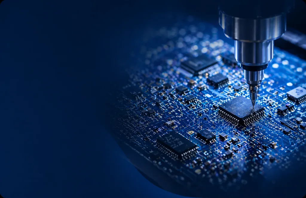
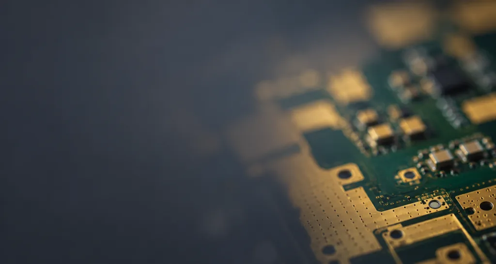
High Frequency PCBs
What is a High Frequency PCB?
High-frequency PCBs are designed for applications that require fast signal transmission, stable electrical performance, and low signal loss. They can be used in both rigid PCB and flexible PCB designs, depending on the product structure and application requirements.
These PCBs often use special high-frequency materials with low dielectric constant (Dk), low dissipation factor (Df), and stable thermal performance. Material selection is important because it directly affects signal integrity, impedance control, and long-term reliability.
High-frequency PCBs are commonly used in HDI PCB designs, high-speed communication equipment, telecommunications systems, RF microwave products, radar systems, antennas, and other advanced electronic applications.
DFYC can support high-frequency PCB fabrication, material selection, stack-up review, impedance control, drilling, lamination, fabrication, assembly, and testing for demanding electronic projects.
Applications for HF PCBs
High-frequency PCBs are used in products that require fast signal transmission, low signal loss, and stable impedance control.
- Telecommunications PCB – antennas, base stations, and wireless modules
- RF & Microwave PCB – RF modules, radar, and microwave systems
- Automotive PCB – LiDAR, ADAS, and vehicle sensors Aerospace & Defense PCB – radar, navigation, and communication systems
- HDI & High-Speed PCB – compact designs and high-speed data transmission
Materials Used for High-Frequency PCBs
High-frequency PCBs require materials with low dielectric constant (Dk), low dissipation factor (Df), low signal loss, and stable thermal performance.
FR-4 is cost-effective for standard PCB manufacturing, but its performance may be limited in high-frequency PCB and RF microwave PCB applications. For demanding designs, materials such as Rogers, Taconic, Isola, Dupont, Panasonic Megtron, Teflon, and flexible substrates are commonly used.
For frequencies above 10GHz, advanced high-frequency PCB materials are recommended to support better signal integrity, lower insertion loss, stable impedance control, and improved environmental reliability.
Learn more about DFYC’s high frequency PCB capabilities:
| Design & Test | Fine trace width and spacing, IPC Class 2 / IPC Class 3 standards, Flying probe testing, AOI inspection, Differential impedance control, TDR testing |
|---|---|
| Drill & Route | Laser drilling, Blind vias, Buried vias, Stacked vias, Back drilling, Countersinks, Counterbores, CNC routing |
| Lamination | 1–32 layer PCB fabrication, Vacuum lamination, Sequential lamination, HDI stack-up processing |
| Plating | Via filling, Edge plating, Castellated holes, ENIG, Immersion Silver, Hard Gold, Lead-Free HASL, OSP |
| Materials | FR-4, Rogers, Taconic, Isola, Panasonic Megtron, High-Speed Materials, RF Microwave Materials, Flex and Rigid-Flex Materials |
| PCB Types | Rigid PCB, Flex PCB, Rigid-Flex PCB, HDI PCB, High-Frequency PCB, Heavy Copper PCB |
| Assembly | SMT Assembly, DIP Assembly, BGA Assembly, Component Sourcing, Programming, Functional Testing |
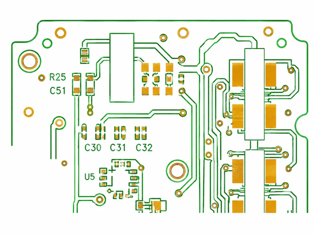
High-Frequency PCB Design
High-frequency PCB design requires the right material selection to support signal speed, impedance control, and low-loss performance.
For cost-sensitive projects, hybrid PCB stack-up designs can be considered. High-frequency materials can be used only on the layers that require better electrical performance, while standard FR-4 can be used for other layers.
This approach helps balance performance, reliability, and manufacturing cost for RF microwave PCB, high-speed PCB, and advanced communication applications.

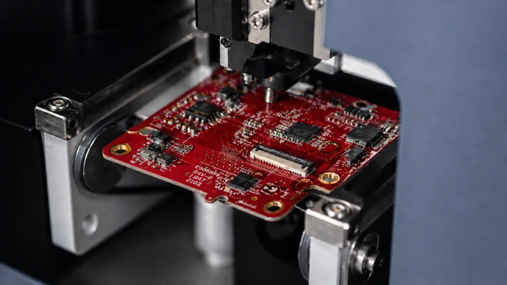
DFYC’s High-Frequency PCB Capabilities
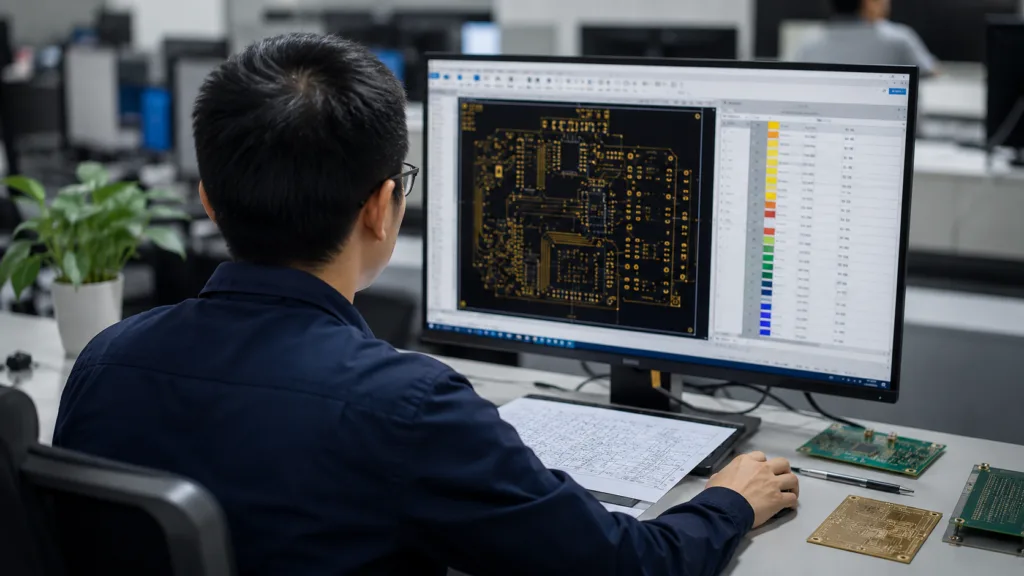
For high-frequency PCB design, material selection and stack-up design are critical to signal performance, impedance control, and long-term reliability. DFYC works with customers to review frequency requirements, material options, and PCB stack-up structures before production.
Our engineering team can support RF microwave PCB fabrication, high-speed PCB design review, controlled-depth drilling, controlled-depth milling, back drilling, laser drilling, impedance control, lamination, plating, assembly, and testing.
DFYC provides one-stop support from PCB layout review and fabrication to PCBA assembly and functional testing. This helps customers reduce design risks, improve manufacturability, and complete complex high-frequency PCB projects more efficiently.
Looking for a High-Frequency PCB Quote?
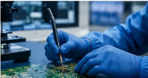
Send us your Gerber files, BOM, fabrication drawings, stack-up details, material requirements, and quantity. Our engineering team will review your files and check the key technical points, including material selection, impedance control, drilling, fabrication, assembly, and testing needs.
After the review, DFYC will provide a clear quotation and useful technical feedback. This helps you understand the production requirements and move your high-frequency PCB project forward with less risk.

Need More Info?
Contact us to discuss your next PCB project.