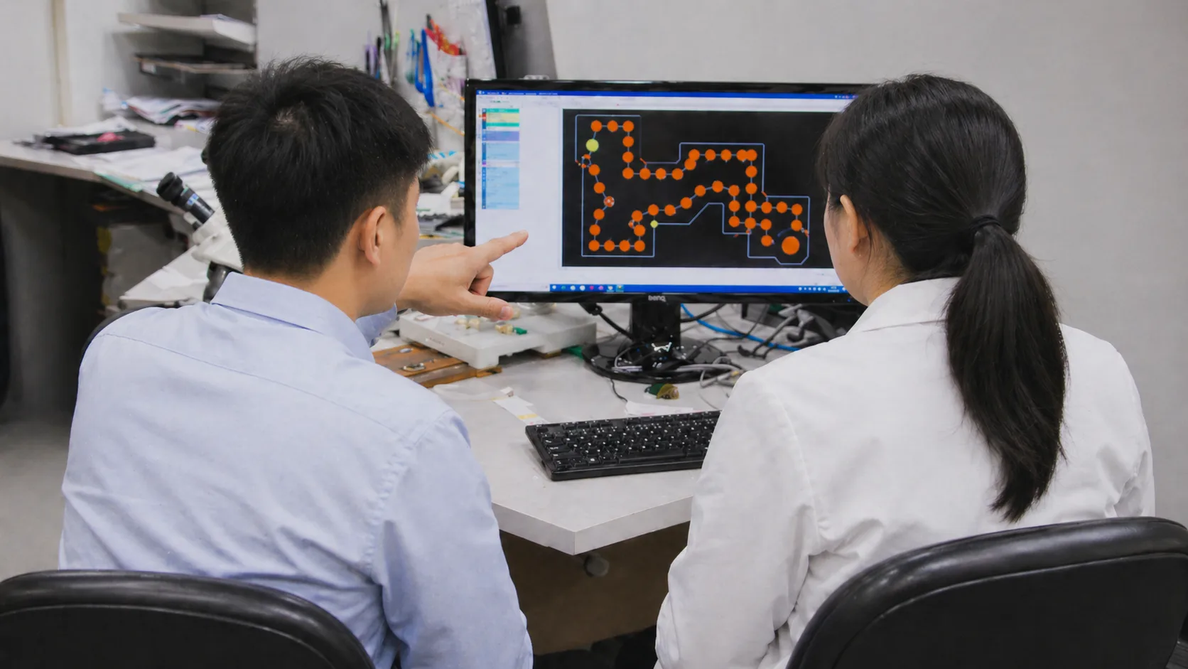
We first review your schematics, component data, board size, and production needs. Our engineers use Altium Designer, Cadence Allegro, and Mentor PADS to place components and route the PCB.
During PCB layout, we check the layer stack-up, impedance, differential pairs, signal paths, power, heat, and assembly needs. We also perform DFM and DFA checks. These checks help us find design problems before production.
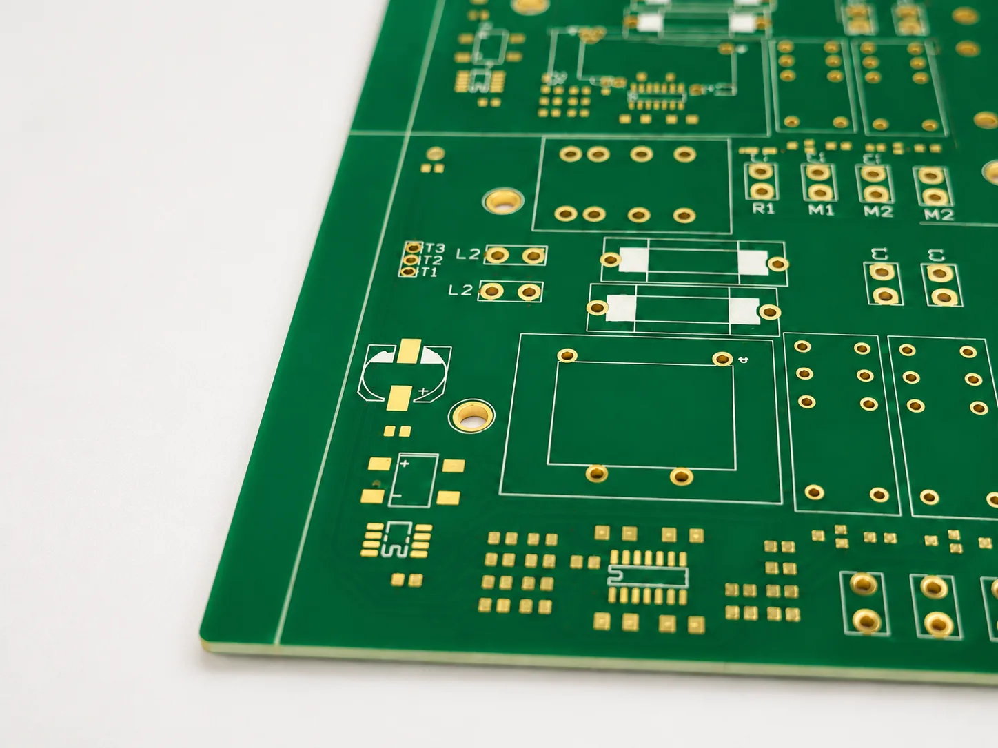
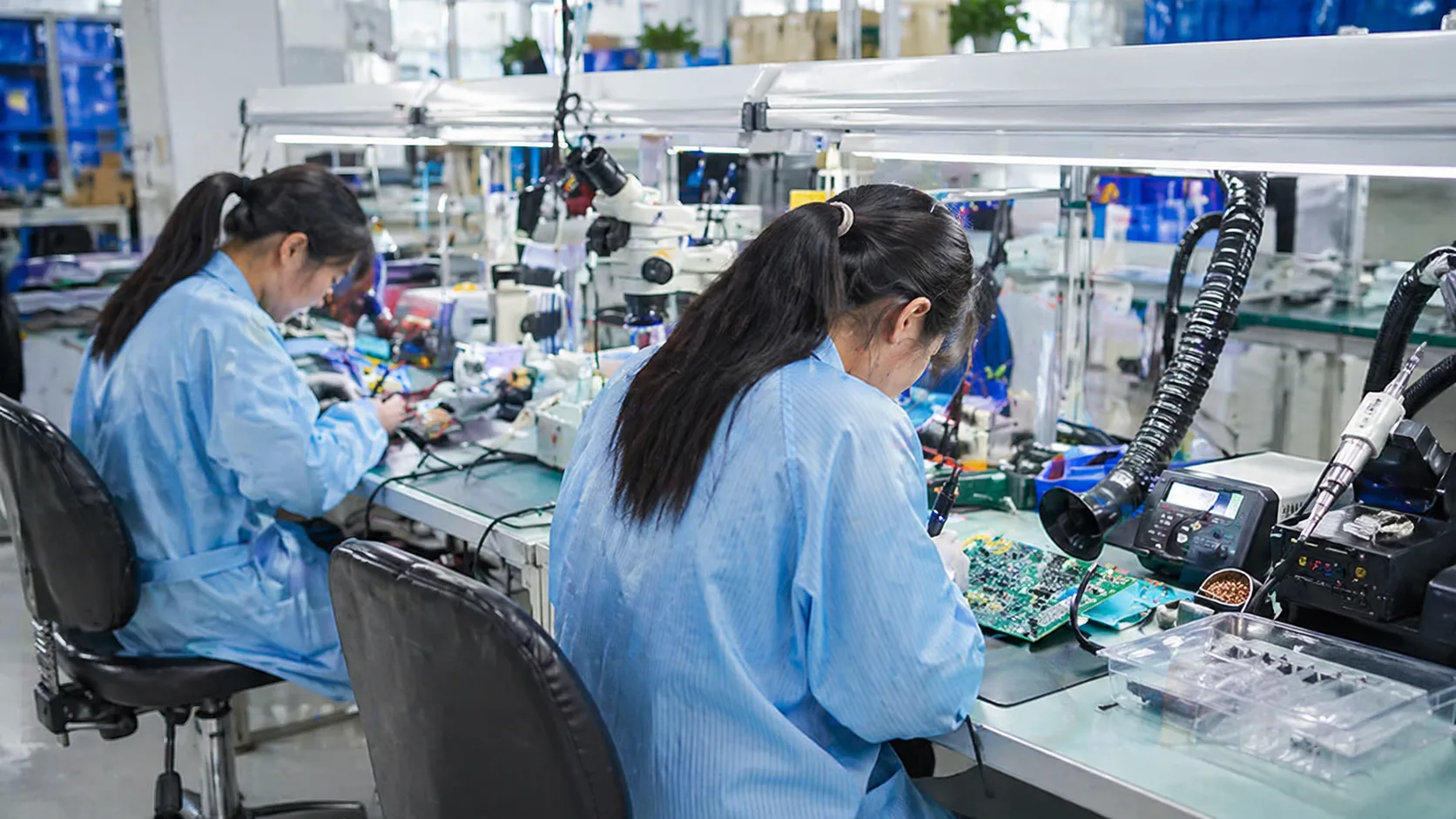
After you approve the layout, we prepare the production files. These files may include Gerber or ODB++, NC drill files, pick-and-place files, fabrication drawings, and assembly drawings. They help move your project from PCB layout to PCB fabrication and assembly.