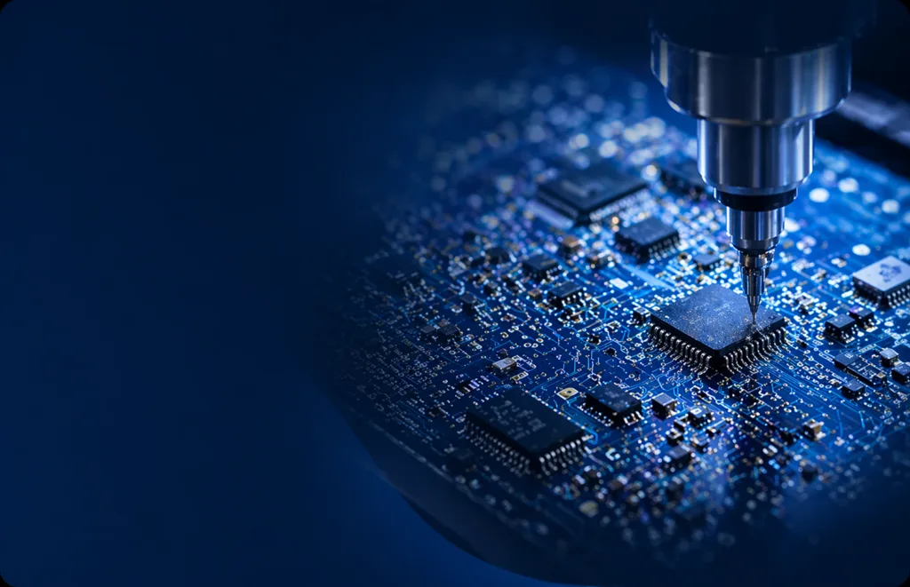
HDI PCB Fabrication & Manufacturing
Trusted HDI PCB Manufacturer Since 2000
Trusted HDI PCB Manufacturer Since 2000
DFYC has provided PCB manufacturing services since 2000. We support complex PCB projects, including HDI PCB fabrication and manufacturing.
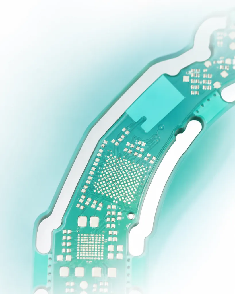
HDI PCBs are used when products need smaller size and higher circuit density. They also help improve electrical performance.
HDI PCBs are common in medical devices, military electronics, aerospace systems, smartphones, tablets, and other digital devices.
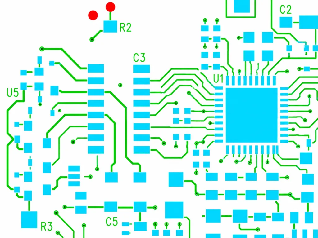
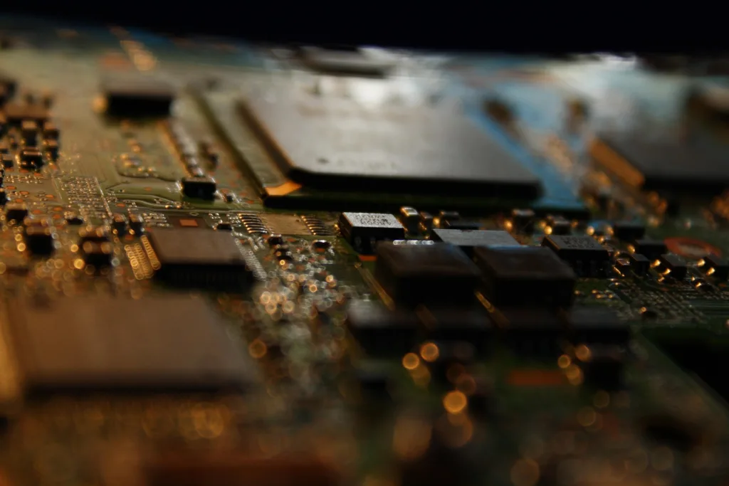
These boards often use fine lines, microvias, blind vias, buried vias, and compact PCB layouts. They are useful for products that need reliable layer-to-layer connections.
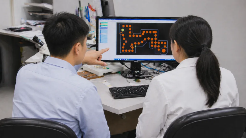
As an HDI PCB manufacturer, DFYC uses advanced production equipment and testing equipment. This helps us control quality, accuracy, and lead time.
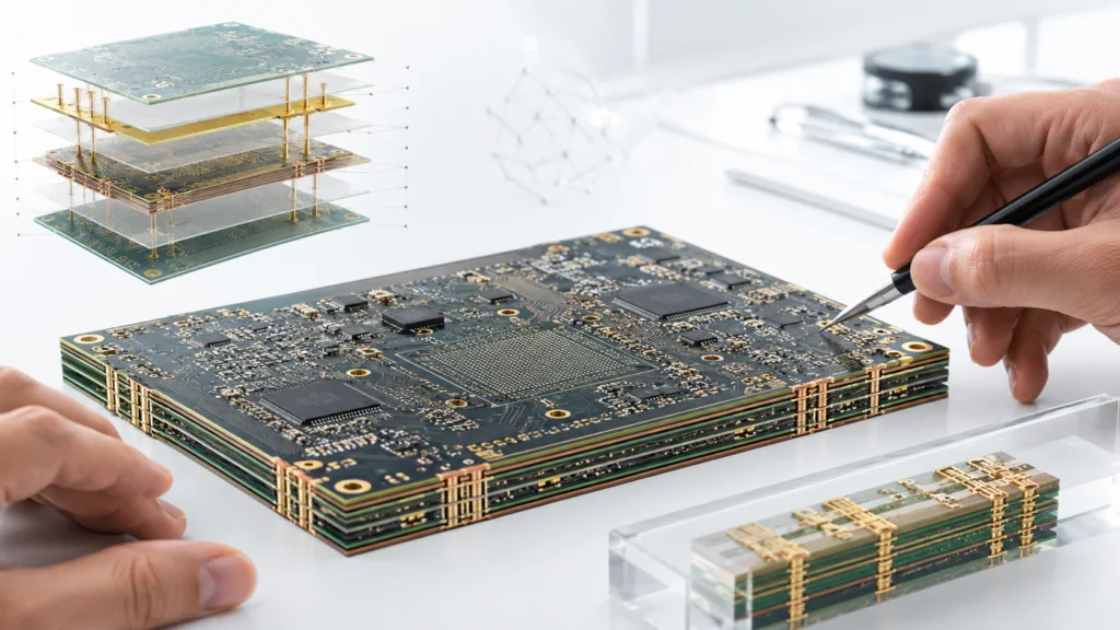
Our engineering team can support HDI PCB materials, stack-up design, microvia structures, impedance control, drilling, lamination, fabrication, and assembly.
From prototype to production, DFYC helps customers complete HDI PCB projects on time and within budget.
HDI Capabilities
HDI PCBs use thin lines, closer spaces, and more dense wiring. This helps create faster connections and reduces the size and weight of the final product.
These boards often include blind vias, buried vias, laser-drilled microvias, sequential lamination, and via-in-pad designs. These features make HDI PCBs suitable for compact and high-performance electronic products.
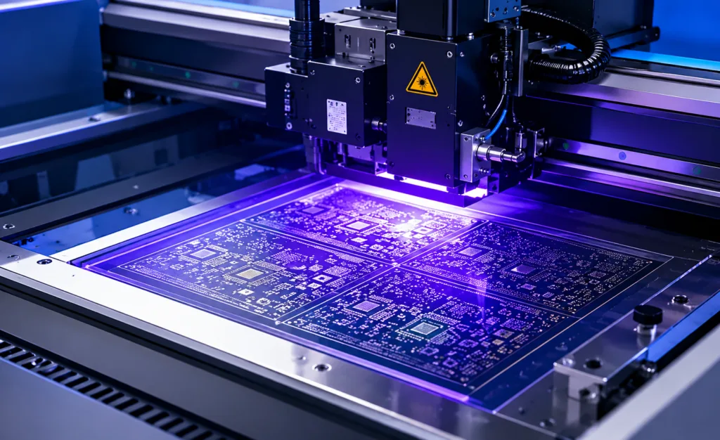
To meet HDI PCB requirements, we use advanced equipment and modern PCB manufacturing technology. This includes laser direct imaging, precise drilling, controlled lamination, and tight tolerance control.
With these processes, DFYC can support complex HDI PCB designs with stable quality, accurate alignment, and reliable electrical performance.d microvias may increase PCB fabrication costs.
Our experienced engineers understand many types of PCB materials and HDI PCB processes. They can answer your technical questions and provide recommendations for material selection, stack-up design, and manufacturability.
They also understand the cost drivers of HDI PCB projects. This helps reduce production risks, control costs, and improve product quality.
Our capabilities also include:
Back drilling
Back drilling helps remove unused parts of a plated through hole. This can reduce signal reflection and improve high-speed signal performance.
Controlled depth drilling / milling
Controlled depth drilling and milling are used when the PCB design requires accurate depth control. This process helps support complex PCB structures and special manufacturing needs.
Buried capacitance
Buried capacitance can improve PCB performance and signal integrity. It uses a very thin dielectric layer to provide distributed decoupling capacitance inside the board.
Hole tolerances
Tight hole tolerances are important for HDI PCB manufacturing. Accurate hole size and hole location help support through-hole connectors, insulation, layer connection, and signal reliability.
Fine pitch
DFYC supports fine pitch designs down to 0.3mm. This is useful for compact components, high-density layouts, and advanced electronic products.
HDI & LDI Technologies
DFYC continues to invest in advanced production equipment, including laser direct imaging (LDI) equipment. LDI technology helps improve imaging accuracy and supports fine lines, close spacing, and high-density PCB designs.
We also support laser processing for blind vias, buried vias, laser-drilled microvias, laser ablated pockets, and precision routing for flex circuits. These processes are important for HDI PCBs and other complex PCB projects.
DFYC can support projects from layout through assembly. Key production steps are handled under one roof. This helps improve communication, control quality, and reduce production risks.
Our engineers keep up with modern PCB manufacturing technologies. They have experience with HDI PCB design, LDI process, microvia structures, lamination, drilling, routing, fabrication, and assembly.
With advanced equipment and engineering support, DFYC helps customers complete HDI PCB projects on time and within budget.
Why Consider DFYC ?
- Custom HDI PCB fabrication for complex and high-density designs
- Fast quoting and engineering review for HDI PCB projects
- Controlled in-house PCB manufacturing under one roof
- Support for fine lines, microvias, blind vias, buried vias, via-in-pad, and sequential lamination
- Practical manufacturing solutions for challenging HDI PCB design and fabrication projects
Client Testimonials
HDI PCB Fabrication Tolerances
Trace Tolerance
+/- .0008″
Internal Drill to Cµ
.007″
Pad Over FHS .004″
.004″
Solder mask clearance over pad size
.005″
From Cµ to the edge of the board
.010″
Impedance
+/- 10%
Board Thickness
+/- 8%
Layer to layer registration +/-
.005″ Lower depending on layer count
Route
+/- .005″ Lower tolerances available
Inside Radius
.015″
Minimum Slot Width
.021″
Drill positioning
.002″
From Cµ to the edge of the board
.010″
Impedance
+/- 10%
Need a PCB fabrication quote?
Submit a form with your project details, including design specifications, quantity, and any special requirements. We’ll take care of the rest.

Need More Info?
Contact us to discuss your next PCB project.