Wire Bonding PCB Services

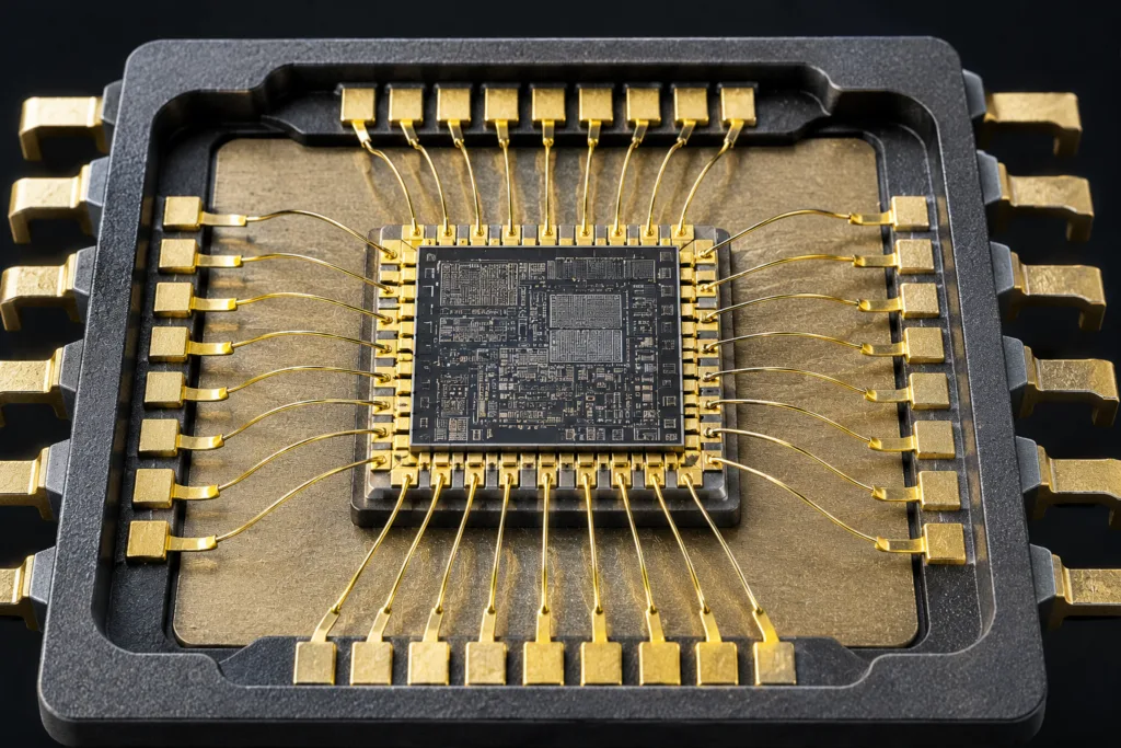
emiconductor die connected to package terminals by gold wire bonding

Wire Bonding Process

Wire bonding creates electrical connections between a semiconductor die and its package, substrate, or PCB. The process uses fine metal wires to connect the chip’s bonding pads to external terminals. Common wire materials include aluminum, gold, and copper.


Advantages of Wire Bonding

Wire bonding provides a reliable way to connect a bare semiconductor die directly to a PCB, substrate, or package. It eliminates the need for a conventional packaged component, which can reduce assembly size and support flexible connection layouts.

This process is useful for compact electronic designs because it supports high connection density, low-profile assemblies, and PCB miniaturization.

Wire Bonding Applications

Wire bonding is used in electronic assemblies that require bare-die connections, compact packaging, or high-density interconnections. Common applications include:

  • Telecommunications equipment
  • Aerospace systems
  • RF and microwave devices
  • Military and defense electronics
  • Medical devices
  • Automotive electronics
  • Consumer electronics
  • Industrial control equipment
  • Energy systems
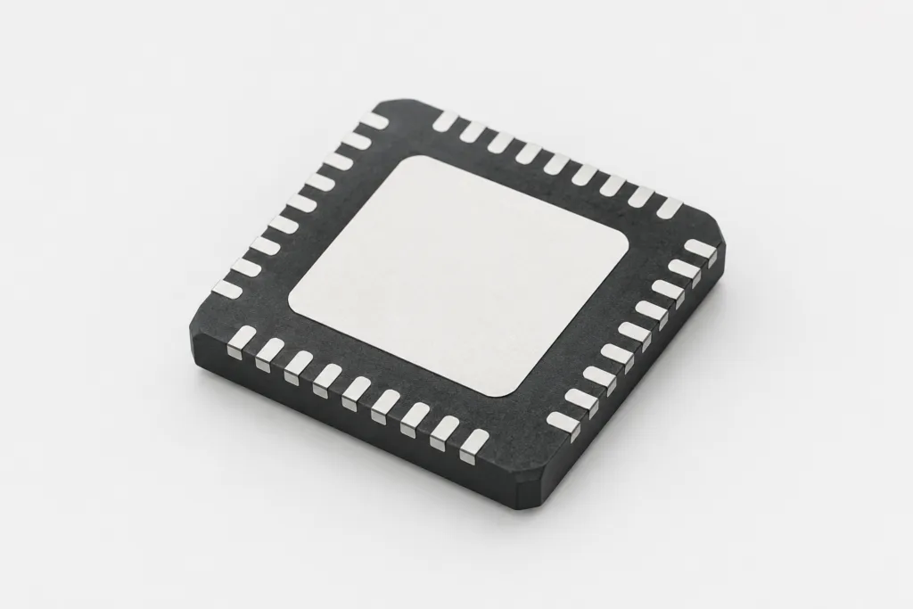
QFN semiconductor package used in wire bonding assembly

Need Wire Bonding Support?

Topline Circuit works with qualified manufacturing partners to provide wire bonding services for suitable PCB and semiconductor assembly projects. Contact us to discuss your design and assembly requirements.
Need a Quote?

We review the design data for every custom PCB and assembly quotation. After receiving your Gerber files, fabrication drawings, schematics, BOM, and other project requirements, our engineering team evaluates the design and prepares a detailed quotation. We respond within 24 hours.

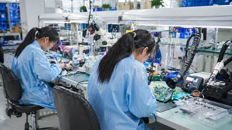
Technicians supporting metal core PCB manufacturing and assembly

Ready to Start Your Project ?

Send us your files. We can help with PCB layout, fabrication, and assembly.