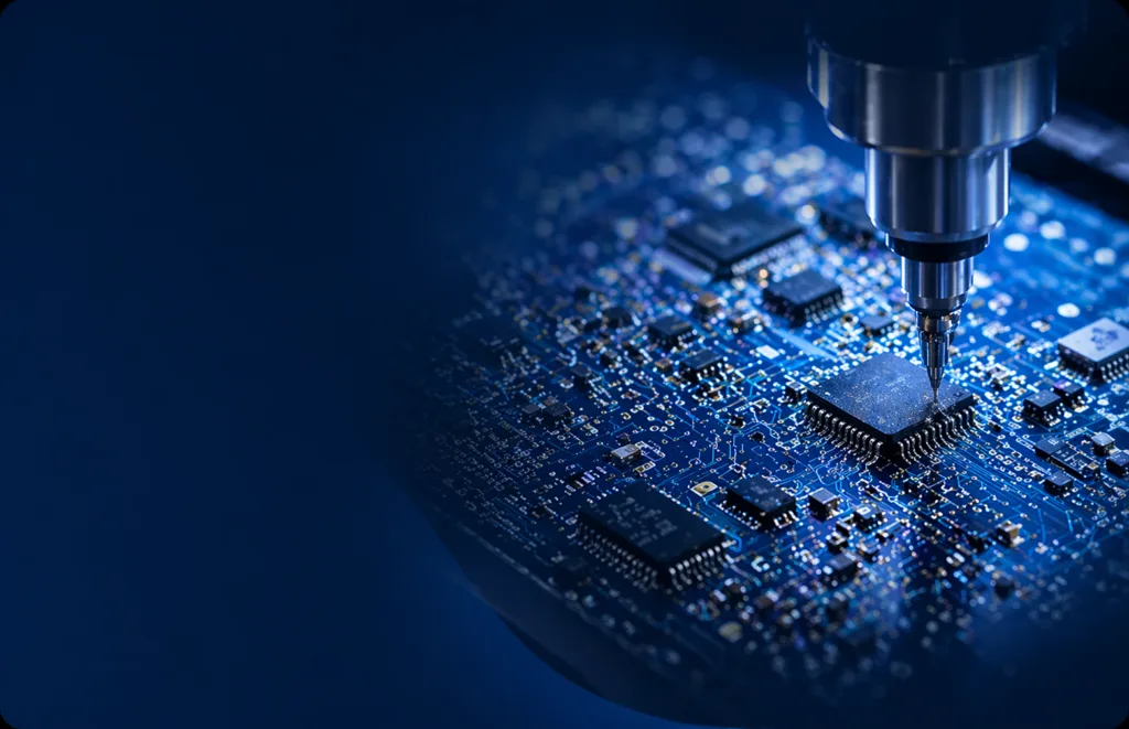
Buried Resistance PCB Manufacturing
Buried Resistance PCB Technology
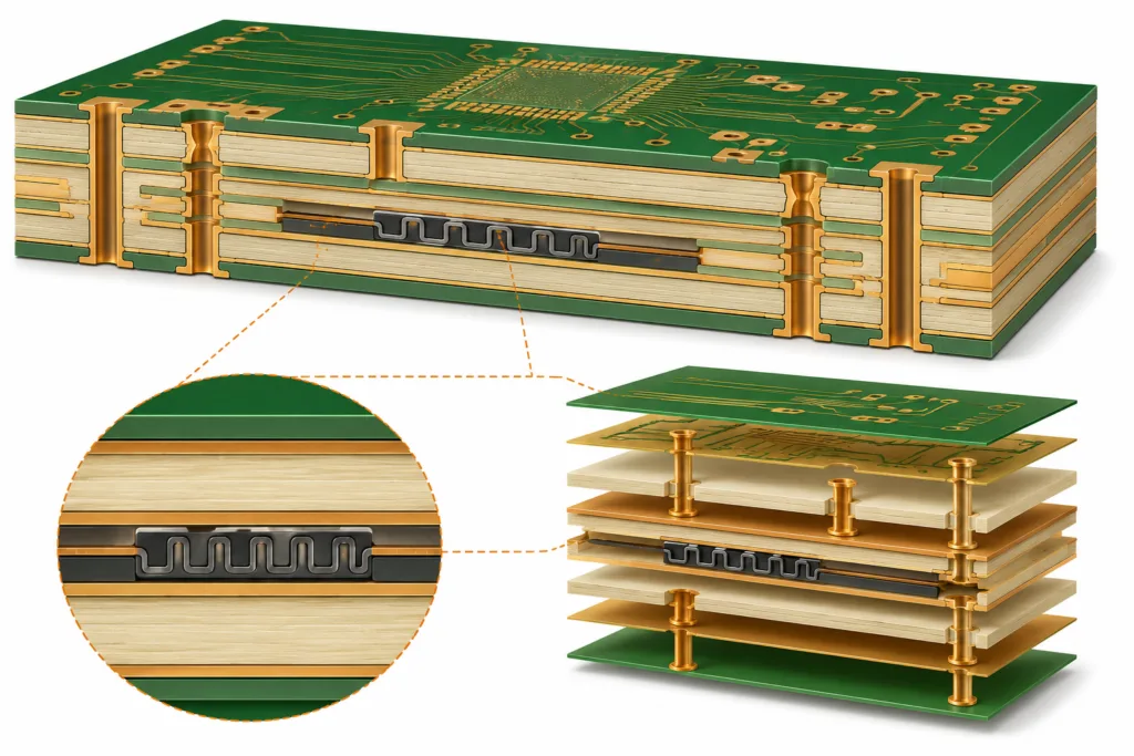
Buried resistance is a special PCB technology that embeds resistors inside the PCB layers. It uses a thin resistive film on a copper nickel phosphorus material to create resistor functions within the board structure.
This technology can help save surface space, reduce discrete components, improve circuit performance, and support compact PCB designs.
Overview of Buried
Resistance in PCBs
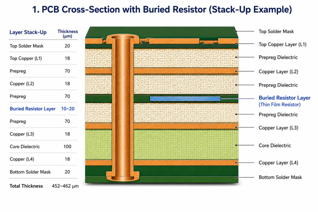
Buried resistors are embedded inside PCB layers to save surface space and keep the board structure compact. They are made by laminating resistive material to a dielectric layer and processing it into planar resistors.
Buried resistance can improve impedance matching, reduce noise, lower cross-talk, and increase PCB reliability.
Key challenges include tight tolerance control during processing and possible resistance value changes during lamination.
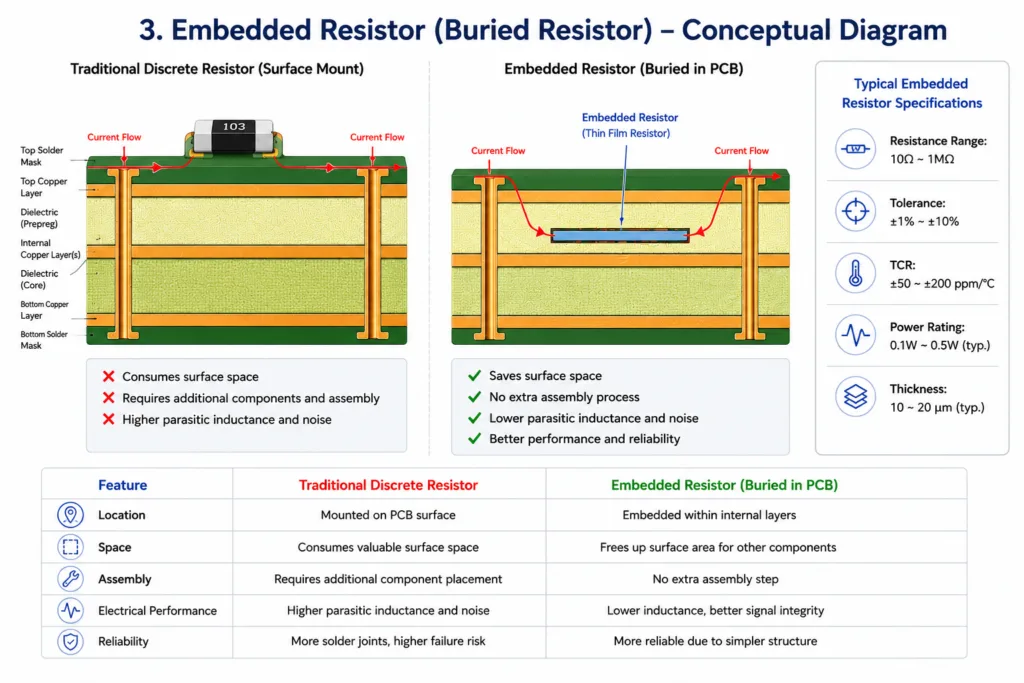
Buried Resistance vs. Traditional Discrete Resistors
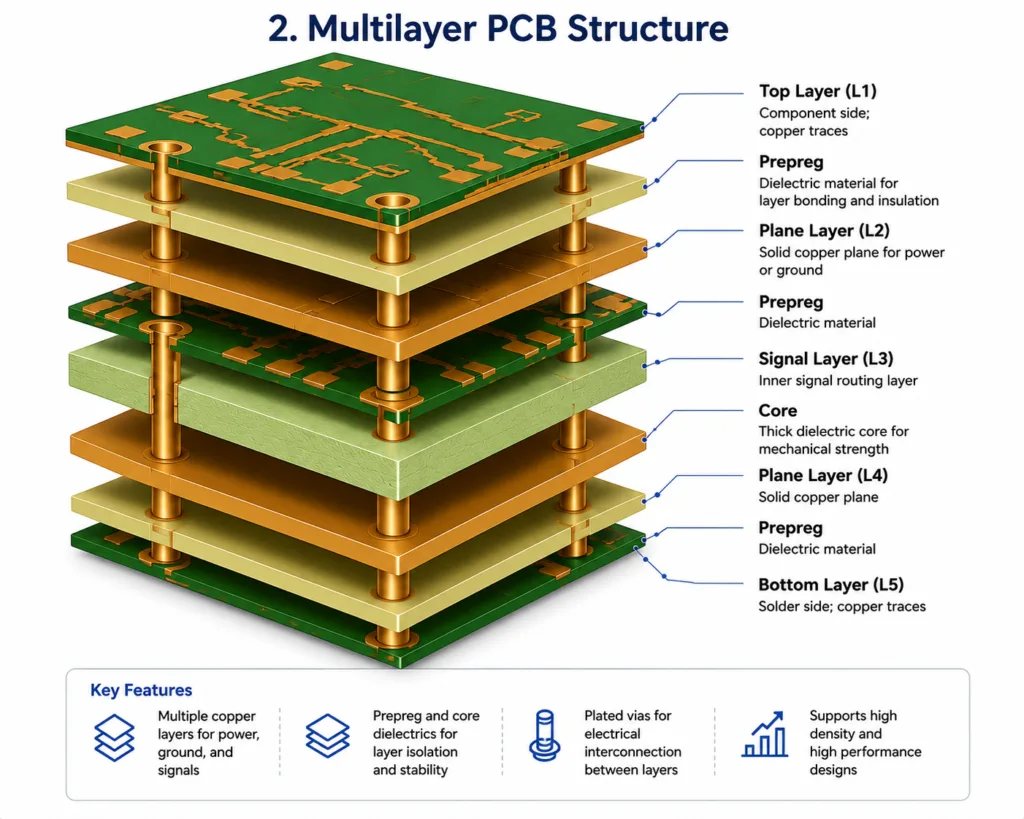
Buried resistance PCB technology helps save board space and improve circuit performance in high-density PCB designs. It is a type of embedded resistor PCB technology. It can reduce the number of surface-mounted components and support compact PCB layouts.
Traditional discrete resistors are mounted on the PCB surface and offer greater flexibility for design changes. Buried resistors free up valuable board space and allow additional components to be integrated into advanced PCB designs.
Applications for PCBs with Buried Resistors
PCBs with buried resistors are used in many industries and electronic applications, including:
- Aerospace
- RF microwave
- Medical devices
- Automotive electronics
- Consumer electronics
- Industrial electronics
- Communication equipment
- Energy systems
Benefits of buried resistance PCB technology include PCB space saving, reduced noise, improved signal integrity, and enhanced circuit performance.
DFYC’s Expertise in PCBs with Buried Resistors
DFYC supports PCB manufacturing with buried resistor technology for compact and high-performance electronic designs. Our engineering team can help review PCB structure, material selection, lamination requirements, and manufacturing feasibility.
We provide advanced PCB fabrication support for buried resistance PCBs, multilayer PCBs, embedded resistor PCB designs, and other custom PCB projects. This helps customers improve space usage, signal integrity, and long-term reliability.
DFYC Is Your Buried Resistance PCB Manufacturer
It is important to work with an experienced PCB manufacturer from the start. DFYC’s engineering team can help review your PCB type, materials, stack-up, buried resistor structure, and design for manufacturability.
DFYC provides custom PCB layout review, PCB manufacturing, PCBA assembly, and engineering support for buried resistance PCBs and other advanced PCB projects. Contact us if you need more information or have questions about your project.
Need a Quote?
We use an efficient review process and engineering analysis to provide a quotation quickly. After you upload your project files, including Gerber files, fabrication drawings, stack-up details, or BOM information, our engineering team will review the data and evaluate the manufacturing requirements so we can better understand your PCB project.

Need More Info?
We can help answer questions about trace width tolerances, PCB stack-ups, material selection, and manufacturing requirements.