Materials

Materials

Materials We Work With

Look no further than DFCY.

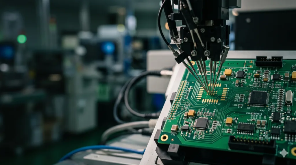
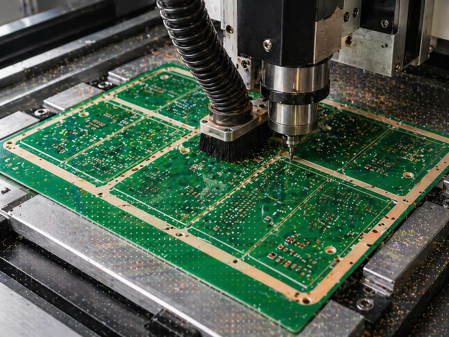
Material selection is an important part of printed circuit board manufacturing. The right material can affect signal integrity, dimensional stability, thermal performance, and long-term reliability.
DFYC works with advanced PCB materials and material combinations to support different design challenges. Our engineering team can help recommend suitable materials for high-speed, high-frequency, high Tg, flex, rigid-flex, and other custom PCB projects.

Our Materials

Materials we work with, and how we help to service their PCB needs.

Arlon high-performance PCB laminate and prepreg materials supplier logo

Arlon
Advanced laminate and prepreg materials for PCB applications.

LEARN MORE
Dupont electronic materials supplier logo for flexible and rigid-flex PCB circuits

DuPont
Comprehensive electronic materials for flex and rigid-flex circuits.

LEARN MORE
Evonik ROHACELL HF material supplier logo for high-frequency PCB applications

Evonik
ROHACELL® HF materials with very low high-frequency absorption.

LEARN MORE
Hanwha ROHACELL HF material supplier logo for high-frequency PCB applications

Hanwha
Low-absorption materials for high-frequency applications.

LEARN MORE
Isola copper-clad laminate and dielectric prepreg materials supplier logo

Isola
Copper-clad laminate and dielectric prepreg solutions.

LEARN MORE
Megtron low-Dk PCB material logo for high-speed and high-frequency circuit boards

Megtron
Low-Dk materials with greater stability than PTFE.

LEARN MORE
Nelco PCB laminate material supplier logo for thermal and mechanical performance

Nelco
Excellent thermal and mechanical performance.

LEARN MORE
OhmegaPly embedded resistor material supplier logo for advanced PCB manufacturing

Ohmega
OhmegaPly materials for buried resistance PCB technology.

LEARN MORE
Panasonic PCB material supplier logo for next-generation electronic technologies

Panasonic
Optimized materials for next-generation PCB technologies.

LEARN MORE
Rogers advanced PCB material supplier logo for wired and wireless communication circuits

Rogers
High-performance materials for wired and wireless communication circuits.

LEARN MORE
Sheldahl thin-film flexible material supplier logo for advanced PCB applications

Sheldahl
Thin-film deposition technology for flex PCB and rigid-flex PCB manufacturing.

LEARN MORE
Taconic engineered composite PCB material supplier logo for advanced circuit boards

Taconic
Advanced composite materials for PCB applications.

LEARN MORE
Tatsuta electronic materials logo for thermal via fill PCB applications

Tatsuta
Materials for thermal via fill applications.

LEARN MORE
ThinFlex polyimide flexible foil substrate supplier logo for flexible PCB manufacturing

ThinFlex
Polyimide flexible foil substrate materials.

LEARN MORE
Ticer thin-film embedded resistor copper foil supplier logo for PCB manufacturing

Ticer
Thin-film copper foil for embedded resistor applications.

LEARN MORE
Ventec copper clad laminate manufacturer logo for professional PCB production

Ventec
Copper clad laminate materials for PCB applications.

LEARN MORE

Free Guide

10 Questions You Should Ask Before Choosing Your PCB Solutions Provider

There are many factors to review when choosing a PCB provider, including engineering capability, certifications, production experience, quality control, and customer support. Before starting your next PCB project, use these 10 questions to help you evaluate the right manufacturing partner.

LEARN MORE
A candid, high-resolution photograph capturing the precision automated inspection process of a green PCB circuit board within a sophisticated electronics manufacturing facility. The image is a detailed close-up shot focusing on a section of a complex, vibrant green multi-layer PCB (Printed Circuit Board) mounted on a precise fixture. On the right side, the intricate green PCB is meticulously populated with numerous SMD components, fine copper traces, vias, capacitors, resistors, and integrated circuits. A high-tech, multi-needle robotic inspection probe head with several fine, sharp metal test probes is actively contacting specific gold-plated test pads on the dense PCB surface with extreme accuracy. The probe head itself is a dark, sophisticated robotic assembly with wires and mechanics. The PCB features dense, sharp details, solder joints, and component markings (labels like C42, R119, U7, J3) clearly visible under focused illumination. The background is a beautifully blurred (heavy bokeh, f/1.8), industrial yet clean workshop environment with blurred machinery, equipment, cables, and ambient lights (soft, dark green and blue tones) of the factory floor, conveying a busy, advanced atmosphere. The left side of the frame remains clear and empty, offering significant, clean negative space (留白) with subtle ambient light for textual overlay against the dark background. The scene is illuminated by focused, moody, high-end production lighting highlighting the glossy PCB traces, components, and the metallic probes. The green PCB has visible copper paths and components (microcontrollers, connectors). The robot arm holding the probe head is dark metal. The focus is critically sharp on the probe tip-to-PCB contact point. The depth of field is very shallow (shallow DOF, natural film grain, ISO 6400, f/2.2, 1/160 sec), with sharp details on the PCB area. The photograph is a realistic, professional shot with an advanced tech aesthetic, shot on a full-frame camera (Sony A9 III, 50mm f/1.4 lens) with natural light and grain, capturing the metallic gleam of probes and PCB components. The image has a cinematic, high-quality, technical texture with rich details, shot at 4K resolution (3840x2160 pixels), capturing the specific texture of the green soldermask and components.