HDI PCB Fabrication & Manufacturing
HDI PCB Manufacturing for Complex, High-Density Designs
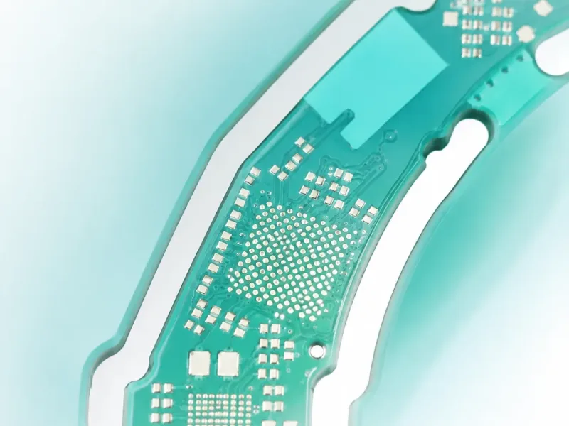
Topline Circuit manufactures HDI PCBs for compact electronic products that require fine-pitch components, dense routing, and reliable interlayer connections. HDI technology uses microvias, blind and buried vias, and thin trace and spacing designs to place more functions within a smaller board area.
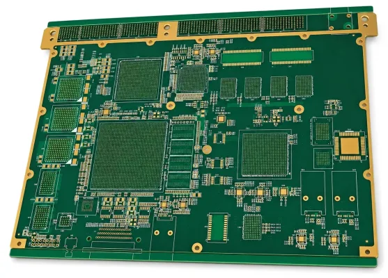
HDI PCBs are widely used in medical devices, communication equipment, industrial control systems, automotive electronics, smartphones, tablets, and other space-constrained products.
Our engineering team reviews the stack-up, microvia structure, materials, impedance requirements, and manufacturing files before production. This helps improve manufacturability and supports reliable PCB fabrication and assembly for complex HDI designs.
HDI PCB Manufacturing Capabilities
HDI PCBs use fine lines and spaces, high-density routing, and compact interconnections to fit more functions into a smaller board area. Common HDI structures include blind and buried vias, laser-drilled microvias, sequential lamination, and via-in-pad designs.
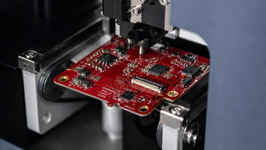
Topline Circuit supports complex HDI fabrication through controlled imaging, drilling, plating, lamination, and registration processes. Our engineering team reviews the stack-up, microvia structure, trace and spacing requirements, and manufacturing data to improve manufacturability and support reliable production.
Additional HDI PCB Capabilities
Our engineering team works with a wide range of PCB materials and HDI structures. We review material selection, stack-up, via design, hole requirements, and other cost drivers to improve manufacturability before production.
HDI and Laser Direct Imaging Technologies
Topline Circuit uses laser direct imaging (LDI) to produce fine traces, tight spacing, and accurate layer patterns for HDI PCBs. Laser processing also supports microvias, blind vias, buried via structures, laser-ablated openings, and precision routing for flexible circuits.
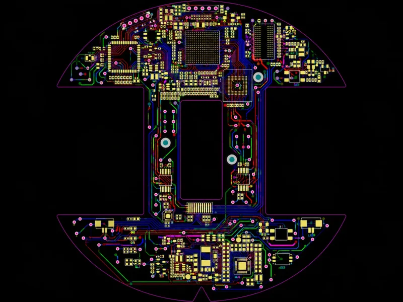
We support the complete process from PCB layout and DFM review to fabrication and assembly. Our engineers review the stack-up, microvia structure, materials, registration, and assembly requirements to improve manufacturability and control potential cost drivers.
Why Choose Topline Circuit?
- Engineering support for complex HDI PCB designs
- DFM review of stack-ups, microvias, fine lines, and via-in-pad structures
- PCB fabrication and assembly support from one supplier
- Process control across drilling, plating, lamination, imaging, and testing
- Material and design review based on electrical, thermal, and assembly needs
- Support for prototypes and production orders
- Clear communication throughout the project
HDI PCB Fabrication Tolerances
Design & Test
Internal Drill to Copper
0.007″
Solder Mask Clearance Over Pad Size
0.004″
From Copper to Board Edge
0.010″
Lamination
Layer-to-Layer Registration
±0.005″
Depending on layer count
Drill & Route
Route
±0.005″
Tighter tolerances available
Minimum Slot Width
0.021″
From Copper to Board Edge
0.010″
Ready to Start Your Project ?
See how our team can support your next PCB project.