Buried Resistance PCB Manufacturing

Buried resistance is a PCB technology that forms thin-film resistors inside the board layers. A nickel-phosphorus (NiP) resistive layer is typically electrodeposited onto copper foil and processed to create the required resistor patterns. Topline Circuit supports buried resistance PCB fabrication with engineering review of the material, stack-up, resistor values, and manufacturing requirements.

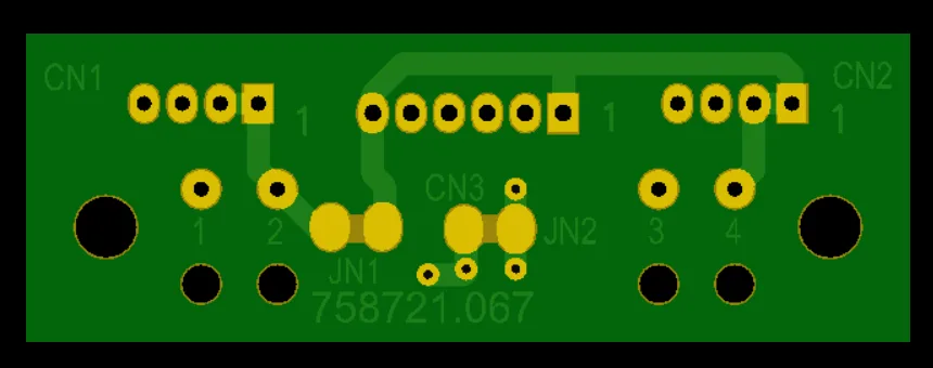
PCB layout with embedded thin-film buried resistor patterns
Buried resistance PCB technology with embedded thin-film resistors

Overview of Buried Resistance in PCBs

Buried resistors are embedded within the PCB layers. They save surface space and reduce the need for surface-mounted resistors without significantly increasing the finished board thickness.

During fabrication, the resistive material is laminated to a dielectric layer and subtractively etched to form planar resistors. The completed resistor layer is then laminated into the PCB stack-up.

Buried resistance can improve impedance matching, reduce noise and crosstalk, and support stable circuit performance. However, tight resistance tolerances can be difficult to maintain during etching and lamination. Processing conditions may also change the final resistor value.

Similarities and Differences Between Buried Resistance and Traditional Discrete Resistors
Buried and discrete resistors perform the same basic electrical function, but they use different construction methods.

Discrete resistors are mounted on the PCB surface. They are available in many values and tolerances and can be replaced after assembly. However, they require surface space, solder joints, and assembly operations.

Buried resistors are formed inside the PCB. They provide more surface space for other components and can shorten electrical paths. Depending on the design and production volume, they may also reduce component placement and assembly requirements.

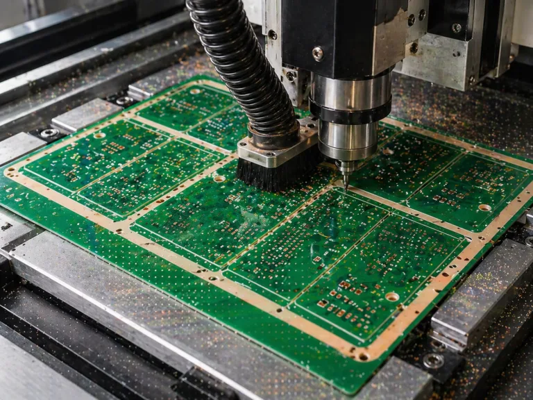
PCB drilling process for buried and discrete resistor board fabrication Select 90 more words to run Humanizer.
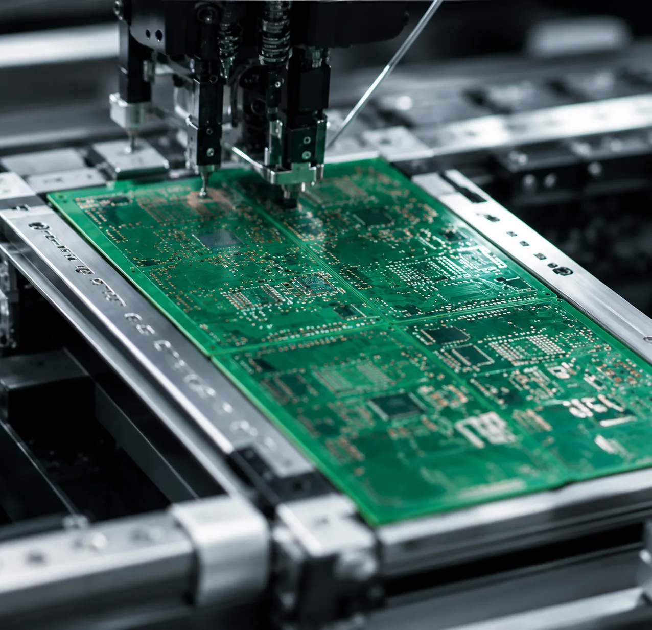
Automated PCB production for buried resistor applications

Applications for PCBs With Buried Resistors

PCBs with buried resistors may be used in a wide range of industries and applications, including:

  • Telecommunications
  • Aerospace electronics
  • RF and microwave circuits
  • Defense electronics
  • Medical devices
  • Automotive electronics
  • Consumer electronics
  • Industrial electronics
  • Energy equipment

The main benefits include better use of board space, fewer surface-mounted passive components, reduced noise, and shorter signal paths.

Topline Circuit’s Experience With Buried Resistor PCBs
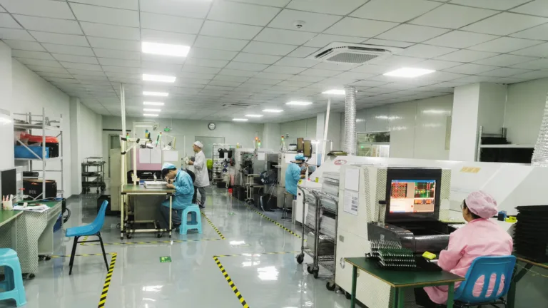
Topline Circuit supports buried resistor PCB projects from file review through fabrication and electrical testing. Our engineering team can review the resistor artwork, target values, tolerances, stack-up, materials, and processing requirements before production.

PCB manufacturing facility supporting buried resistor board production Select 92 more words to run Humanizer.
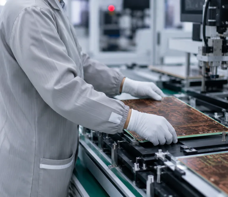
PCB manufacturing technician handling circuit boards in production

Topline Circuit Is Your Buried Resistance PCB Manufacturer

Buried resistor PCB fabrication requires careful control of material selection, resistor geometry, etching, lamination, and testing. Early engineering review can help identify design and manufacturing risks before production.

Ready to Start Your Project ?

Send us your files. We can help with PCB layout, fabrication, and assembly.