
Custom PCB Fabrication, Manufacturing &
Assembly
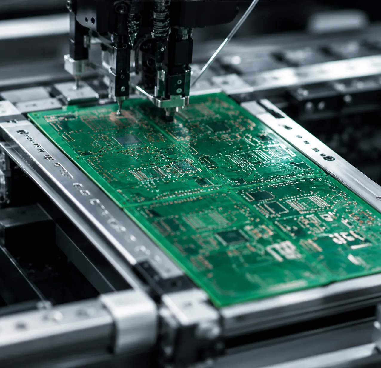
Automated PCB production for buried resistor applications

Extensive Custom PCB & Concurrent Engineering Expertise

Topline Circuit provides custom PCB manufacturing services for complex projects. We support PCB fabrication, assembly, and engineering services.

Our engineers have rich experience with PCB materials and manufacturing processes. We help customers choose the right materials, improve designs, and reduce production risks.

Through concurrent engineering, we work with customers from the early design stage.

We provide DFM suggestions and practical solutions to improve quality and control costs.

Topline Circuit supports PCB projects from prototypes to mass production with reliable processes and experienced engineering teams.

Custom PCB Manufacturing Capabilities

Topline Circuit has strong custom PCB manufacturing capabilities supported by advanced equipment and experienced engineers.

We maintain a wide range of PCB materials to support different project requirements and reduce production delays.

Our engineering and manufacturing teams have experience with various PCB materials and structures.

We help customers select suitable materials, solve technical challenges, and improve PCB designs for better manufacturability.

With reliable processes and professional support, Topline Circuit delivers custom PCB solutions for prototypes and production projects.

Automated optical inspection and precision custom PCB manufacturing machine

Why Choose Topline Circuit?

  • RF and microwave PCB fabrication
  • Engineering support for design and manufacturing questions
  • DFM review before production
  • Material, stack-up, and impedance review
  • PCB fabrication, component sourcing, and assembly
  • ISO 9001 and UL certified

Custom PCB Fabrication Tolerance Capabilities

Topline Circuit continuously invests in advanced PCB manufacturing equipment and process control technologies to achieve reliable fabrication accuracy and tight PCB tolerances for prototype and production requirements.

Trace Tolerances

Trace Width / Spacing Tolerance
±0.0008″
Internal Drill to Copper
0.007″
Pad Over Finished Hole Size
0.005″
Solder Mask Clearance Over Pad Size
0.004″
Copper to Board Edge
0.010″
Controlled Impedance Tolerance
±10%

Lamination

Finished Board Thickness Tolerance
±8%
Layer-to-Layer Registration
±0.005″
Depending on layer count

Drill & Route

Routing Tolerance
±0.005″
Tighter tolerances available
Inside Radius
0.015″
Minimum Slot Width
0.021″
Drill Position Accuracy
0.002″
Copper to Board Edge
0.010″
Controlled Impedance Tolerance
±10%

Need a Custom PCB Quote?

Technicians supporting metal core PCB manufacturing and assembly

Ready to Start Your Project ?

Send us your files. We can help with PCB layout, fabrication, and assembly.