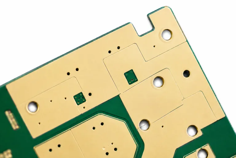
High Frequency PCBs

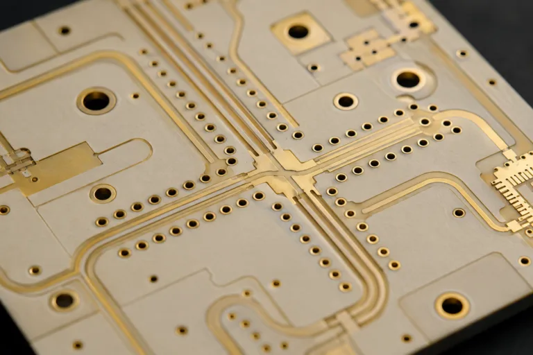
High frequency PCB with gold RF traces and via fences

What Is a High Frequency PCB?

A high frequency PCB is a printed circuit board designed to carry high-frequency signals with low signal loss and stable impedance. It may use a rigid, flex, or rigid-flex structure, depending on the product design and operating environment.

Unlike a standard PCB, a high frequency PCB requires careful material selection and tighter control of the stack-up, trace geometry, copper surface, and manufacturing process. High frequency PCB materials usually have a stable dielectric constant (Dk), a low dissipation factor (Df), and controlled thermal expansion. These properties help reduce signal loss, impedance variation, and performance changes caused by heat.

High frequency PCBs are commonly used in RF and microwave systems, telecom equipment, wireless communication devices, radar systems, satellite electronics, and high-speed data products. Material properties, operating frequency, impedance requirements, thermal conditions, and PCB structure should all be reviewed before fabrication.

High Frequency PCB Applications

High frequency rigid, flex, and rigid-flex PCBs are used in

  • RF microwave systems
  • telecom equipment
  • wireless devices
  • radar and LiDAR systems
  • antenna systems
  • aerospace electronics
  • high-speed data products

These applications require low signal loss, stable impedance, and reliable signal transmission.

Gold-plated PCB for aerospace electronic applications
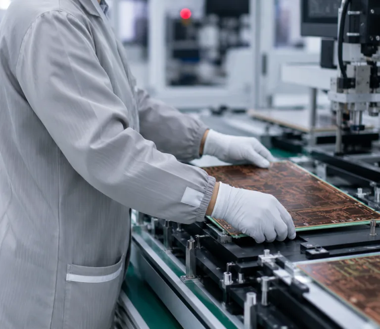
PCB manufacturing technician handling circuit boards in production

High Frequency PCB Materials

Material selection is important for high frequency PCB performance. The right laminate depends on the operating frequency, signal loss, impedance requirements, thermal conditions, board structure, and application environment.

FR-4 may support some less demanding designs. Low-loss and PTFE-based laminates are often selected for RF, microwave, radar, antenna, telecom, and high-speed applications. High frequency flex designs may also require low-loss flexible materials.

Common material manufacturers include Rogers, Isola, Taconic, Panasonic Industry, and DuPont. Material availability and processing requirements should be confirmed before production.

High Frequency PCB Manufacturing Capabilities

Review our fabrication options for high frequency, RF, microwave, and mixed-material PCB projects. Final specifications are confirmed during the DFM and quotation review.

Engineering & Testing

2 mil trace width, 3 mil air gap, IPC Class 2 and IPC Class 3, flying probe netlist testing, differential impedance, TDR testing, and automated optical inspection (AOI)

Drilling & Routing

Countersinks and counterbores, scoring, rout-and-retain, laser routing, blind and buried vias, and stacked vias

Lamination

1–30 layers, vacuum lamination, and sequential lamination

Plating & Surface Finishes

Conductive and non-conductive via fill, plated edges, castellated holes, plated milling cutouts, hard gold, soft bondable gold, ENIG, immersion silver, lead-free HASL, and OSP

PCB Materials

Flex and rigid-flex materials, adhesive and adhesiveless polyimide, RF and high-speed laminates, mixed FR-4/PTFE constructions, metal-backed boards, and heavy copper rigid and rigid-flex boards

High Frequency PCB Design

High frequency PCB design requires careful control of material selection, stack-up, impedance, trace geometry, and signal loss. The laminate should match the operating frequency, electrical requirements, thermal conditions, and application environment.

For some projects, a mixed-material stack-up can balance performance and cost. Low-loss materials are used only for critical signal layers, while suitable FR-4 materials are used for the remaining layers. The material combination and lamination process must be reviewed before fabrication.

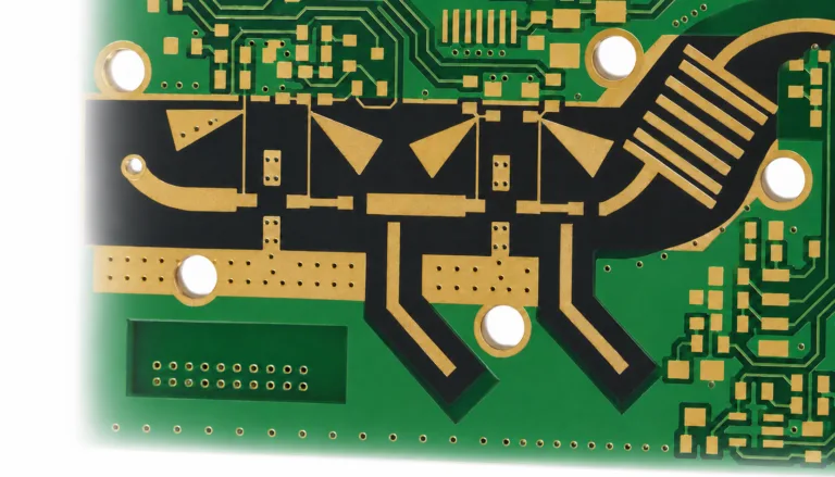
High frequency PCB with microstrip lines and impedance matching structures
Engineers reviewing high frequency PCB layout and signal integrity data

Engineering Support for High Frequency PCBs

High frequency PCB projects require close coordination between the design engineer and PCB manufacturer. Material selection, stack-up, impedance, trace geometry, drilling, and signal loss should be reviewed before production.

Topline Circuit supports controlled-depth drilling, controlled-depth milling, back drilling, and mixed-material PCB construction. Our engineering team can review the design, identify manufacturing risks, and help confirm the appropriate materials and stack-up.

We support projects from PCB layout and fabrication to component sourcing and assembly. This coordinated process helps reduce communication gaps and keeps the design requirements consistent throughout production.

Ready to Start Your Project ?

Send us your files. We can help with PCB layout, fabrication, and assembly.