X-Ray PCB Inspection Services

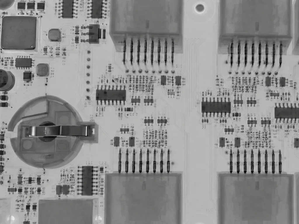
X-ray inspection image showing hidden solder joints on a PCB assembly

Topline Circuit uses X-ray inspection to examine hidden solder joints beneath ball grid array (BGA) packages. This process helps identify defects such as voids, solder bridges, insufficient solder, and misaligned connections between the solder balls and PCB pads. X-ray inspection is part of our quality control process for verifying BGA assembly quality.

Overview of X-Ray PCB Inspection Services

Topline Circuit uses X-ray inspection to evaluate hidden solder joints and internal assembly connections that cannot be checked through visual inspection alone. 

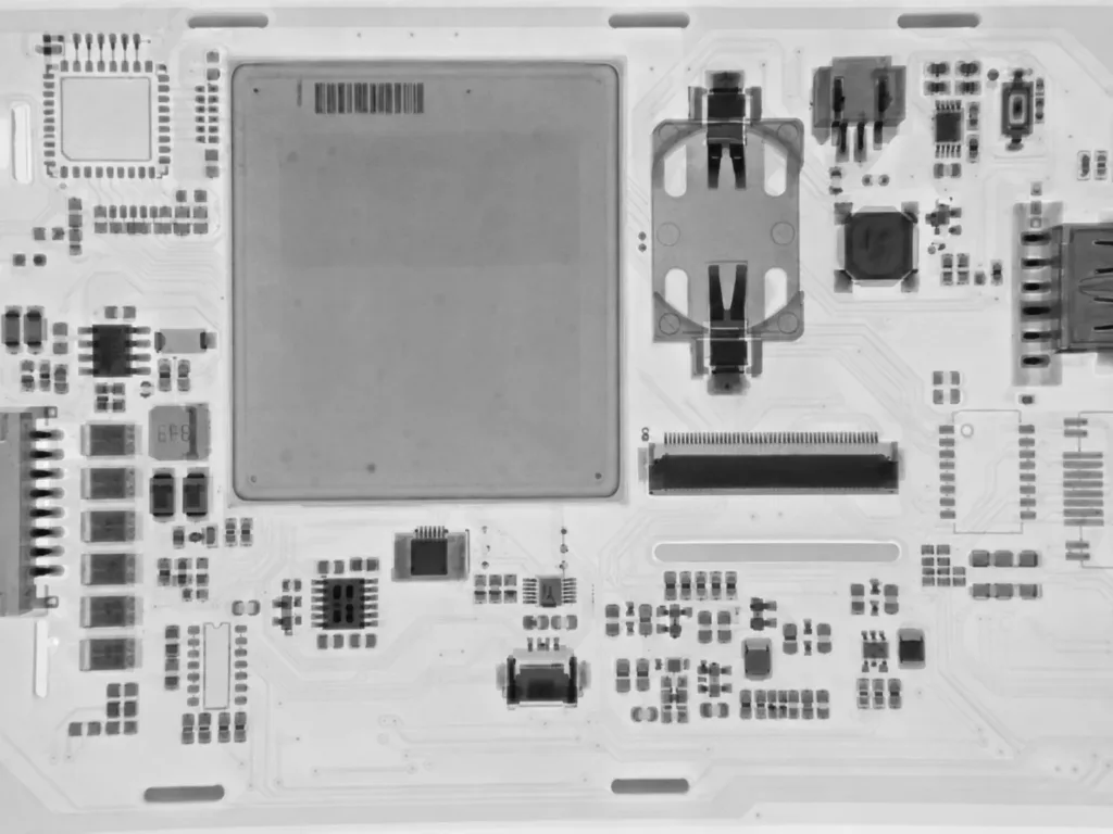
The process provides consistent inspection results and helps detect voids, solder bridges, open connections, misalignment, and other assembly defects.

X-ray PCB inspection showing hidden solder joints and internal connections

AOI vs. X-Ray PCB Inspection

Automated optical inspection (AOI) uses cameras to examine visible solder joints, component placement, polarity, alignment, and surface defects. It checks the assembled board against defined inspection criteria.

X-ray inspection examines solder joints and connections hidden beneath components, including BGA, QFN, and other bottom-terminated packages. It is used to detect internal defects that AOI cannot see, such as voids, solder bridges, open joints, and insufficient solder.

X-Ray PCB Inspection Applications

X-ray inspection is used for PCB assemblies with hidden solder joints, high-density components, or demanding quality requirements. Common applications include:

  • Telecommunications equipment
  • Aerospace systems
  • RF and microwave devices
  • Military and defense electronics
  • Medical devices
  • Automotive electronics
  • Consumer electronics
  • Industrial control equipment
  • Energy systems


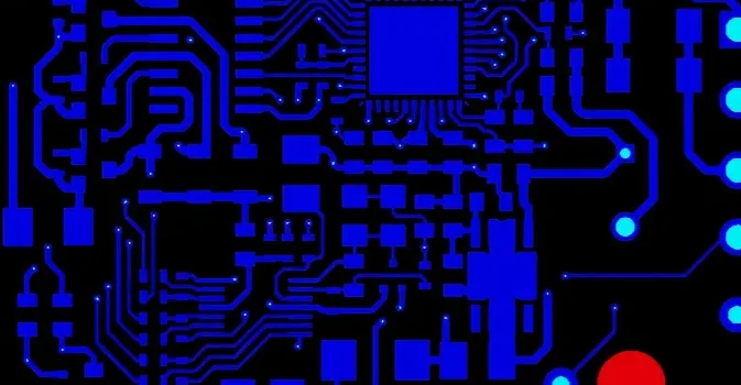
PCB layout engineering review with component placement, routed traces, and plated vias

Your PCB Manufacturing and Assembly Partner

Topline Circuit supports PCB projects from layout and material selection through fabrication, assembly, inspection, and testing. Our engineering team reviews stack-ups, component requirements, and manufacturability factors before production.

X-ray inspection supports our quality control process by verifying hidden solder joints and identifying internal assembly defects. Contact us to discuss your PCB fabrication and assembly requirements.

Need a Quote?

We review the design data for every custom PCB and assembly quotation. After receiving your Gerber files, fabrication drawings, schematics, BOM, and other project requirements, our engineering team evaluates the design and prepares a detailed quotation. We respond within 24 hours.

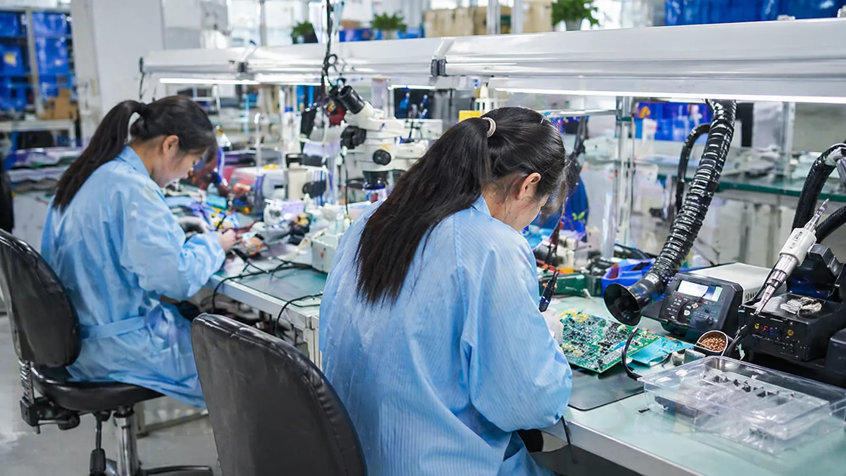
Technicians supporting metal core PCB manufacturing and assembly

Ready to Start Your Project ?

Send us your files. We can help with PCB layout, fabrication, and assembly.