
PCB Assembly Requirements for RF and Telecom Communication Boards
RF and telecom communicat

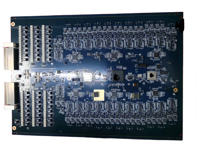
RF and telecom communication boards need more than standard PCB assembly. These projects often include fine-pitch SMT parts, RF shields, BGA packages, dense routing, and functional testing requirements. Buyers should review the BOM, pick-and-place file, assembly drawing, inspection scope, and test plan before production release. Clear PCB assembly requirements help the supplier review risk early and reduce questions during quotation and production planning.
RF and telecom boards often combine signal-sensitive circuits with dense PCBA structures.
A standard control board may focus on basic placement and solder quality. An RF communication board may need tighter attention to component position, shield placement, connector direction, and test coverage.
A small error can create a large problem. A wrong capacitor value can affect circuit behavior. A shifted RF shield can affect mechanical fit. A hidden solder joint issue under a BGA can escape normal visual inspection.
Buyers should not treat telecom PCB assembly as a simple placement job. They should define the assembly scope before the RFQ.
A good review should cover:
These points help the supplier review the project with fewer assumptions.
Different communication products need different assembly checks.
A compact RF module may use small passives, RF shields, and fine-pitch ICs. A communication gateway may need connectors, programmed devices, and functional testing. A telecom control board may need BOM sourcing control and stable test coverage.
| Hardware Type | Main Assembly Risk | Buyer Check |
|---|---|---|
| RF module | Fine-pitch placement and shield fit | Check SMT and shield notes |
| Telecom control board | BOM and functional test gaps | Confirm part data and test method |
| Communication gateway | Connectors and mixed components | Review assembly drawing |
| RF front-end board | Signal-sensitive component placement | Check placement and polarity |
| Communication backplane | Connector alignment | Review mechanical notes |
| High-density PCBA | Hidden solder joints | Confirm X-ray scope |
The hardware type should guide the assembly plan. A single generic checklist is not enough for all communication boards.
The BOM controls the assembly result.
RF and telecom PCBA projects may use filters, oscillators, RF connectors, shield cans, BGA ICs, small passives, and programmed devices. These parts need clear and complete data.
A useful BOM should include:
A missing package size can create placement risk. An unclear substitute rule can delay sourcing. A missing RF shield part can change the assembly scope.
Turnkey PCB Assembly needs stronger BOM control. The supplier manages component sourcing in this model. Buyers should approve substitute rules before purchasing starts.
Consigned assembly also needs clean BOM data. The buyer supplies the parts, but the supplier still needs correct labels, quantities, and reference designators.
RF telecom assembly needs consistent files.
Gerber files show the board layout. The pick-and-place file controls component location. The assembly drawing explains polarity, orientation, shield notes, and special handling.
These files must use the same revision.
A placement file from an older revision can create the wrong assembly. A BOM from another revision can cause part mismatch. An assembly drawing without polarity notes can create orientation risk.
PCB design review should check footprint match, pad design, test access, and component clearance. These checks reduce assembly questions before production starts.
The file package should include:
A supplier should ask questions before assembly starts. Early questions are safer than rework after production.
Most RF and telecom boards rely on SMT Assembly.
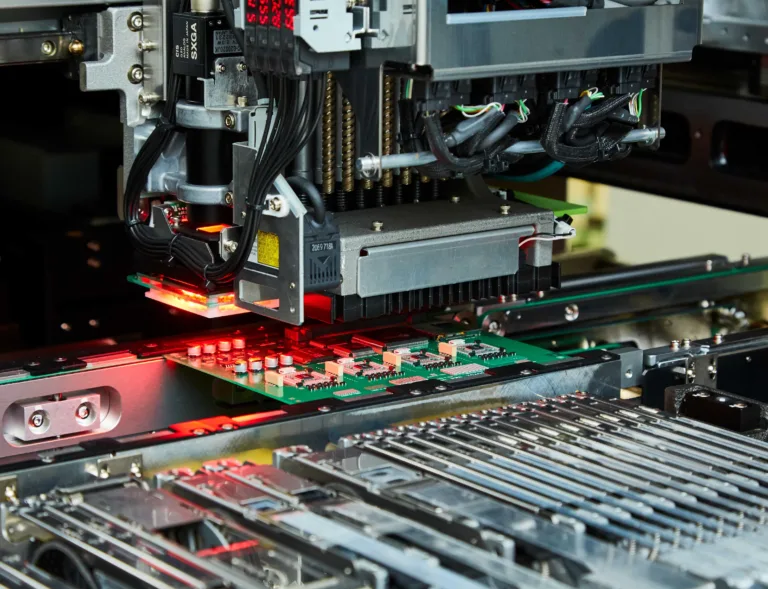
SMT quality affects solder paste, placement, reflow, and inspection. Dense communication boards may use small passives, fine-pitch ICs, QFN packages, and BGA devices.
The supplier should review SMT risk from the actual project files.
A general SMT answer is not enough for a dense telecom board. The supplier should explain risk based on package type, layout density, and inspection access.
RF shields and connectors need clear instructions.
An RF shield may affect mechanical fit, inspection access, and final assembly. A connector may affect signal path, mating direction, and mechanical alignment.
The assembly drawing should show shield position, connector direction, height limits, and any manual assembly steps. These details should not be left to production judgment.
Buyers should check these questions:
These checks help the supplier plan the Assembly Process. They also help buyers avoid missing assembly scope in the quotation.
Many RF and telecom boards use BGA, QFN, LGA, or bottom-terminated packages.
These packages support dense layouts. They also create hidden solder joint risk. AOI cannot fully inspect solder joints under a BGA.
BGA Assembly should be reviewed before production if the project uses hidden joints.
Buyers should confirm:
Hidden solder joint risk should be handled before production release. It should not become a problem after assembly.
Inspection should match the PCBA design.
A simple telecom control board may need AOI and visual inspection. A dense RF module may need SPI, AOI, X-ray, and functional testing. A BGA design may need X-ray inspection before test.
Assembly Capabilities should be checked when the project has multiple inspection needs.
| Inspection Method | What It Checks | When It Matters |
| SPI | Solder paste position and volume | Fine-pitch SMT parts |
| AOI | Visible placement and solder defects | Most SMT assemblies |
| X-ray | Hidden solder joints | BGA, QFN, LGA packages |
| Visual inspection | Connectors and special parts | Mixed assembly projects |
| ICT | Electrical checks | Boards with test access |
| Functional testing | Board operation | Telecom control and RF modules |
| First article review | First build confirmation | New projects and revisions |
“Inspection included” is not a clear scope. Buyers should confirm what each inspection method covers.
Testing is important for telecom PCB assembly.
Many communication boards need firmware, interface checks, power input checks, RF-related validation, or product-level testing. The supplier cannot quote these steps correctly without test information.
Buyers should prepare:
Functional testing is different from assembly inspection. AOI checks visible assembly quality. Functional testing checks whether the board works as required.
The test scope should be clear before PCBA processing starts.
Prototype assembly helps buyers find risks before batch production.
A prototype RF telecom board may reveal BOM issues, footprint errors, shield fit problems, test access gaps, or firmware problems. These findings should be reviewed before the next build.
Prototype PCB Assembly is useful when the design still needs validation.
After prototype assembly, buyers should review:
A prototype order should not be treated as only a sample. It should help the buyer prepare a more stable production release.
Two quotations may look similar. They may include different work.
One supplier may include BOM review, SMT assembly, AOI, X-ray, programming, functional testing, and reports. Another supplier may include only placement and basic inspection.
Buyers should compare the full scope.
| Quotation Item | Why It Matters | Buyer Check |
| BOM review | Finds sourcing and packaging issues | Confirm part data and substitutes |
| SMT assembly | Controls placement and solder risk | Check fine-pitch and reflow needs |
| RF shield assembly | Affects hardware fit | Confirm shield notes |
| BGA inspection | Finds hidden joint risk | Confirm X-ray scope |
| Functional testing | Confirms board operation | Provide test procedure |
| Reports | Support traceability | Ask what records are provided |
A low price may miss important assembly work. A clear scope helps buyers compare suppliers fairly.
Some telecom projects use backplanes.
A Communication Backplane PCB Board may use large connectors, multilayer structures, thick boards, and strict mechanical alignment. These projects need separate assembly review.
Backplane assembly checks may include:
Backplane projects should not be handled like small SMT modules. The supplier should review both the board structure and connector assembly needs.
A complete file package helps the supplier quote the project correctly.
Incomplete files force suppliers to make assumptions. These assumptions can create price gaps, scope gaps, and production questions.
Buyers should prepare:
These files help the supplier review PCB assembly requirements with fewer assumptions.
RF and telecom communication boards need careful assembly review.
Buyers should check the BOM, placement data, assembly drawing, inspection scope, and test plan before release. They should also confirm SMT risk, BGA inspection, RF shield notes, connector requirements, and functional test coverage.
A complete review helps reduce assembly questions. It also helps the supplier plan the correct production scope.
For engineering review and quotation support, please send your Gerber files, BOM, pick-and-place file, assembly drawing, RF shield notes, testing requirements, and quantity requirements to sales@toplinecircuit.com.
Our team can help you evaluate the board structure, materials, component assembly, and testing requirements based on your product’s operating environment and performance needs.

RF and telecom communicat

Choosing a PCBA manufactu