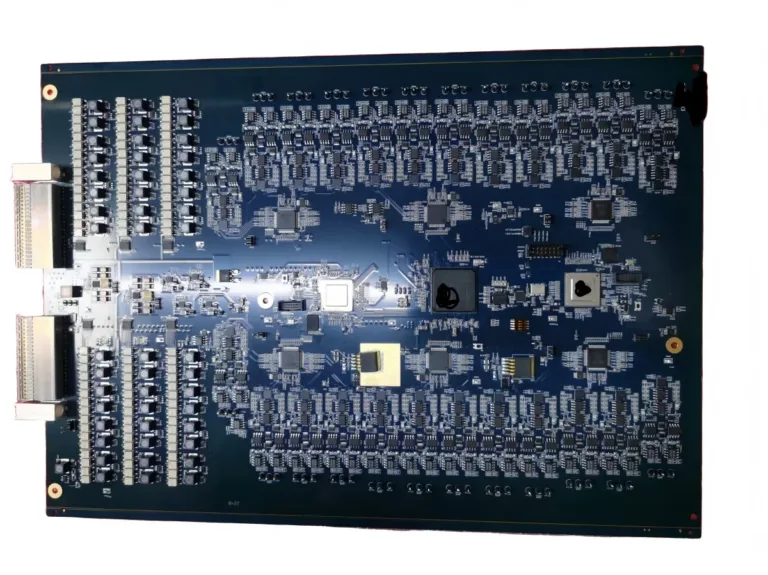
PCB Assembly Requirements for RF and Telecom Communication Boards
RF and telecom communicat



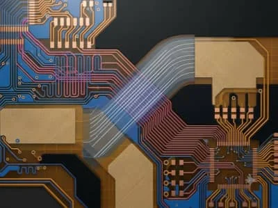
As 5G communication systems continue to evolve toward higher data rates, lower latency, and greater integration, the importance of PCB stack-up design has become increasingly prominent. The layer stack-up structure not only determines signal transmission paths within the board but also directly affects impedance control, crosstalk levels, and overall electromagnetic compatibility.
With the gradual adoption of millimeter-wave applications, traditional two-dimensional routing can no longer meet the stability requirements of high-frequency signals. Therefore, optimizing 5G performance through scientific stack-up design has become a key direction in high-speed PCB engineering.
A well-designed stack-up can effectively reduce signal loss, improve return path integrity, and provide a stable electrical foundation for complex multilayer systems.

In high-speed and high-frequency environments, stack-up design is not only about circuit connectivity but also about building a stable signal transmission environment.
The design objectives of 5G PCB stack-up focus on the following aspects:
In practical engineering, stack-up structure directly defines the performance ceiling of a 5G PCB.
A scientific design must comprehensively consider materials, power distribution, and signal relationships.
Different application scenarios require different stack-up structures, balancing performance and cost.
| Stack-Up Type | Structural Features | Application Scenario | Performance Characteristics |
| Symmetrical Stack-Up | Balanced signal and ground layers | Base stations | High stability and strong EMI resistance |
| Hybrid Reference Structure | Alternating power and ground layers | Communication modules | Balanced cost and performance |
| High-Frequency Optimized Structure | Multi-ground + microstrip design | Millimeter-wave applications | Low signal loss |
| High-Density HDI Structure | Multiple blind/buried vias | Compact terminals | High integration density |
In real PCB development, stack-up design must be optimized through simulation and process control.
The key lies in fine control and system-level matching.
With the rapid advancement of 5G communications, PCB stack-up design has evolved from traditional circuit layout into a system-level engineering discipline. A well-optimized stack-up structure significantly enhances signal integrity, electromagnetic compatibility, and overall system stability, enabling low-loss transmission even in complex multilayer environments. As millimeter-wave and even higher-frequency technologies continue to develop, stack-up design will further move toward higher precision and greater integration, becoming an indispensable foundation for future 5G and next-generation communication systems.
RF and telecom communicat
Choosing a PCBA manufactu