PCB Assembly Requirements for RF and Telecom Communication Boards
RF and telecom communicat


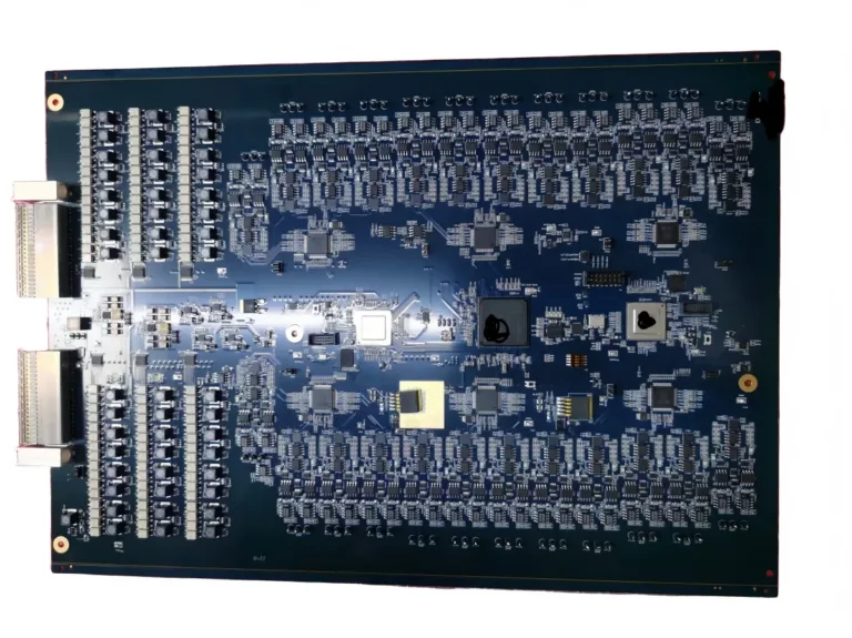
Against the backdrop of continuous upgrades to data centers and high-performance network infrastructure, core switches, routers, and NVMe storage devices are jointly driving the evolution of high-speed interconnect architectures towards higher bandwidth and lower latency. The PCBs of these devices are no longer just traditional signal bearer boards, but core physical platforms carrying 112G or even 224G PAM4 high-speed signals, requiring them to maintain signal integrity and system stability under extremely high frequency environments. Simultaneously, the explosive growth of data traffic has made long-distance link transmission, increased port density, and multi-channel concurrency the norm, placing more stringent demands on PCB layer stack-up structures, material selection, and process control. Breaking down the layer structure, key processes, and high-speed signal challenges helps to more systematically understand the design logic and technical priorities of PCBs for this type of high-end network equipment.
Application Scenarios Concentrated in Core Network and High-Speed Storage Systems
In modern data center architectures, these devices undertake critical data exchange and storage tasks.
The increasing speed of applications necessitates PCB designs focused on maximizing bandwidth and stable transmission capabilities.
Layer counts are concentrated in high-density designs ranging from 12 to 24 layers
Structural design must balance high-speed signal and power integrity.
This stack-up structure provides a stable physical foundation for high-speed links.
Back-drilling has become a crucial means of improving high-speed signal quality
Structural interference needs to be effectively controlled during high-speed signal transmission.
This process significantly improves the stability and consistency of high-speed links.
112G/224G PAM4 and Crosstalk Suppression: Core Design Challenges
In ultra-high-speed signal environments, signal integrity becomes a critical constraint.
Signal control capabilities in high-speed environments directly determine the upper limit of system performance.
Long-Link Loss Control: A Crucial Guarantee for Stable System Operation
In large-scale data center interconnects, signal transmission distances increase significantly.
Loss control capabilities determine the system’s reliability under high-load scenarios.
Comparison Table of Key Technologies for Core Switches / Routers / NVMe Storage PCBs
| Dimension | Core switch/router PCB | NVMe storage PCB | Technical Focus |
| Application Positioning | High-speed network forwarding and interconnection | High-speed storage access | Bandwidth and delay control |
| Layer Structure | 16–24 floors | Layers 12–20 | Signal and power separation |
| High-Speed Signals | 112G/224G PAM4 | PCIe/NVMe high-speed channels | Signal integrity |
| Process Requirements | Backplane design + back-drilling process | High-density, high-speed cabling | Reflection and loss control |
| Crosstalk Control | Multi-port parallel transmission | Multi-channel storage access | EMI and crosstalk suppression |
| Long-Link Performance | Long-distance transmission in data centers | Internal interconnects of storage arrays | Insertion loss optimization |
The PCB design of core switches, routers, and NVMe storage devices is continuously evolving towards ultra-high speed, high density, and high reliability. The core challenges lie in 112G/224G PAM4 signal processing capabilities and stable transmission control in long-link environments. As data centers expand and network bandwidth continues to increase, PCBs not only need to support more complex wiring structures but also require multi-dimensional optimization in materials, processes, and electrical design. A systematic analysis of layer structure, key processes, and high-speed signal challenges provides a clearer understanding of the core value of this type of PCB in modern network and storage systems, and offers a clear reference direction for subsequent high-end interconnect designs.
RF and telecom communicat
Choosing a PCBA manufactu